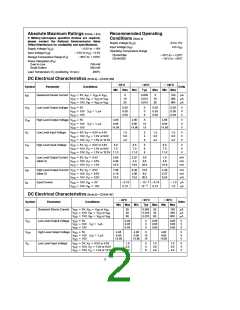
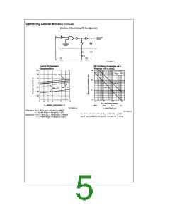
DC Electrical Characteristics (Note 2)ÐCD4541BC (Continued)
b
a
a
85 C
40 C
§
25 C
§
§
Symbol
Parameter
Conditions
Units
Min Max Min
Typ
Max Min Max
e
e
e
e
0.5V or 4.5V
V
High Level Input Voltage
V
V
V
5V, V
O
3.5
7.0
3.5
7.0
3
6
9
3.5
7.0
V
V
V
IH
OL
OH
IN
DD
DD
DD
e
10V, V
15V, V
1.0V or 9.0V
O
e
1.5V or 13.5V 11.0
11.0
11.0
O
e
e
e
e
0.4V
I
I
I
Low Level Output Current
(Note 3)
V
DD
V
DD
V
DD
5V, V
2.32
3.18
12.4
1.96
2.66
10.4
3.6
9.0
1.6
mA
mA
mA
O
e
e
10V, V
15V, V
0.5V
1.5V
2.18
8.50
O
O
34.0
e
e
e
e
2.5V
High Level Output Current
(Note 3)
V
DD
V
DD
V
DD
5V, V
5.1
4.27
2.25
8.8
130
8.0
3.5
mA
mA
mA
O
e
e
10V, V
15V, V
9.5V
2.69
10.5
1.85
7.22
O
O
13.5V
30.0
b
5
e
e
e
e
b
b
b
b
Input Current
V
V
15V, V
15V, V
0V
0.3
10
10b
0.3
1.0
mA
mA
DD
IN
5
15V
0.3
0.3
1.0
DD
IN
e
e
50 pF (refer to test circuits)
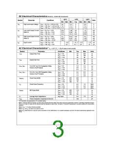
AC Electrical Characteristics* T
25 C, C
§
A
L
Symbol
Parameter
Conditions
Min
Typ
Max
Units
e
e
e
t
t
t
t
t
f
t
Output Rise Time
V
V
V
5V
50
30
25
200
100
80
ns
ns
ns
TLH
DD
DD
DD
10V
15V
e
e
e
Output Fall Time
V
DD
V
DD
V
DD
5V
50
30
25
200
100
80
ns
ns
ns
THL
10V
15V
e
e
e
t
PLH, PHL
Turn-Off, Turn-On Propagation Delay,
8
Clock to Q (2 Output)
V
DD
V
DD
V
DD
5V
1.8
0.6
0.4
4.0
1.5
1.0
ms
ms
ms
10V
15V
e
e
e
t
PHL, PLH
Turn-On, Turn-Off Propagation Delay,
16
V
DD
V
DD
V
DD
5V
3.2
1.5
1.0
8.0
3.0
2.0
ms
ms
ms
Clock to Q (2 Output)
10V
15V
e
e
e
Clock Pulse Width
V
DD
V
DD
V
DD
5V
400
200
150
200
100
70
ns
ns
ns
WH(CL)
CL
10V
15V
e
e
e
Clock Pulse Frequency
MR Pulse Width
V
DD
V
DD
V
DD
5V
2.5
6.0
8.5
1.0
3.0
4.0
MHz
MHz
MHz
10V
15V
e
e
e
V
DD
V
DD
V
DD
5V
400
200
150
170
75
ns
ns
ns
WH(R)
10V
15V
50
C
C
Average Input Capacitance
Any Input
5.0
7.5
pF
pF
I
Power Dissipation Capacitance (Note 4)
100
PD
*AC Parameters are guaranteed by DC correlated testing.
Note 1: ‘‘Absolute Maximum Ratings’’ are those values beyond which the safety of the device cannot be guaranteed. Except for ‘‘Operating Temperature Range’’
they are not meant to imply that the devices should be operated at these limits. The table of ‘‘Electrical Characteristics’’ provides conditions for actual device
operation.
e
Note 2: V
0V unless otherwise specified.
SS
Note 3: I
and I are tested one output at a time.
OL
OH
Note 4: C determines the no load AC power consumption of any CMOS device. For complete explanation, see 54C/74C family characteristics application note
PD
AN-90.
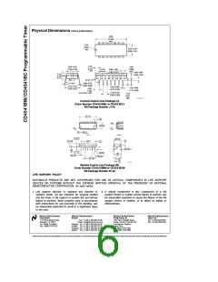
3

 NSC [ National Semiconductor ]