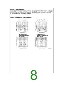
Special Considerations
In certain applications the external load-resistor current may
include both V and signal-line components. To avoid
DD
s l
25 C, or 0.4V at T 25 C (calcu-
A
not exceed 0.6V at T
lated from R
§
§
A
values shown). No V
current will flow
DD
ON
drawing V current when switch current flows into IN/OUT
DD
pin, the voltage drop across the bidirectional switch must
through R if the switch current flows into OUT/IN pin.
L
Typical Performance Characteristics
‘‘ON’’ Resistance as a
Function of Temperature for
‘‘ON’’ Resistance vs Signal
e
b
e
V 15V
EE
Voltage for T
25 C
§
V
DD
A
‘‘ON’’ Resistance as a
Function of Temperature for
‘‘ON’’ Resistance as a
Function of Temperature for
b
e
b
e
V 5V
EE
V
V
EE
10V
V
DD
DD
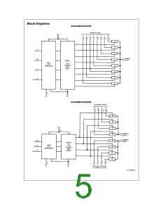
TL/F/5662–5
8

 NSC [ National Semiconductor ]