e
e e
t 20 ns, unless otherwise specified.
f
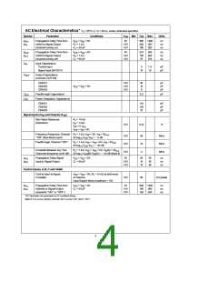
AC Electrical Characteristics* T 25 C, t
§
A
r
Symbol
Parameter
Conditions
V
DD
Min Typ
Max
Units
e
e
e
e
t
t
Propagation Delay Time from
Inhibit to Signal Output
(channel turning on)
V
V
0V
5V
600 1200
ns
ns
ns
PZH,
EE
SS
1 kX
50 pF
R
10V
15V
225
160
450
320
PZL
L
L
C
e e
V
SS
t
t
Propagation Delay Time from
Inhibit to Signal Output
(channel turning off)
V
0V
5V
210
100
75
420
200
150
ns
ns
ns
PHZ,
EE
e
e
R
1 kX
10V
15V
PLZ
L
L
C
50 pF
C
IN
Input Capacitance
Control input
5
7.5
15
pF
pF
Signal Input (IN/OUT)
10
C
OUT
Output Capacitance
(common OUT/IN)
CD4051
CD4052
CD4053
10V
10V
10V
30
15
8
pF
pF
pF
e
e
0V
V
EE
V
SS
C
C
Feedthrough Capacitance
0.2
pF
IOS
Power Dissipation Capacitance
PD
CD4051
CD4052
CD4053
110
140
70
pF
pF
pF
Signal Inputs (V ) and Outputs (V
IS
)
OS
e
Sine Wave Response
(Distortion)
R
10 kX
L
e
f
IS
1 kHz
10V
0.04
%
e
V
V
5 V
p-p
IS
e
e
V
SI
0V
EE
e
20 log
e
e
0V, V 5V
IS p-p
eb
3 dB
Frequency Response, Channel
‘‘ON’’ (Sine Wave Input)
R
L
1 kX, V
EE
,
10V
10V
10V
40
10
3
MHz
MHz
MHz
V
/V
10 OS IS
e
20 log
e
e
e
5V
IS
Feedthrough, Channel ‘‘OFF’’
R
1 kX, V
EE
V
0V, V
,
p-p
L
SS
eb
V
/V
10 OS IS
40 dB
e
20 log
e
e
e
Crosstalk Between Any Two
Channels (frequency at 40 dB)
R
1 kX, V
EE
V
SS
0V, V (A) 5V
IS
L
p-p
eb
V
10 OS
(B)/V (A)
IS
40 dB (Note 3)
e
e
e
0V
t
t
Propagation Delay Signal
Input to Signal Output
V
V
5V
25
15
10
55
35
25
ns
ns
ns
PHL
EE
SS
50 pF
C
10V
15V
PLH
L
Control Inputs, A, B, C and Inhibit
e
e
e
0V, R 10 kX at both ends
Control Input to Signal
Crosstalk
V
V
EE
of channel.
Input Square Wave Amplitude 10V
SS
L
10V
65
mV (peak)
e
e
e
e
0V
t
t
Propagation Delay Time from
Address to Signal Output
(channels ‘‘ON’’ or ‘‘OFF’’)
V
V
5V
500 1000
ns
ns
ns
PHL,
EE
SS
50 pF
C
10V
15V
180
120
360
240
PLH
L
*AC Parameters are guaranteed by DC correlated testing.
Note 3: A, B are two arbitrary channels with A turned ‘‘ON’’ and B ‘‘OFF’’.
4

 NSC [ National Semiconductor ]