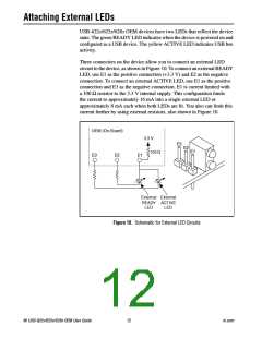
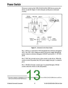
Power Switch
The power switch on the USB-622x/625x/628x OEM device powers the
device on and off. Figure 11 shows the pins on the power switch and
circuitry.
100 kΩ
to Ground
VDC Out
VDC In
3
2
1
J4/J6/J8
SW1
Switch
NC NC
100 kΩ
Outer
Shell
J4/J6/J8
XF1
SW1
2
1
Power to
Device
Power
Connector
FUSE
3
100 kΩ
Figure 11. Schematic for the Power Switch
Pin 1, VDC In, is connected to VDC through the fuse (reference designator
XF1). The VDC is the voltage provided by the power supply through the
power connector (reference designator J4/J6/J81) and must be 11–30 VDC,
20 W.
Pin 2, VDC Out, provides power to the circuitry on the device. When the
switch is in the On position, the VDC power supply from pin 1 is routed to
pin 2.
Pin 3, 100 kΩ to Ground, connects pin 2 to ground through a 100 kΩ
resistor when the switch is in the Off position.
1
The power connector is designated as J4 on USB-6225/6255 OEM devices, J6 on USB-6221/6229 OEM devices, and J8 on
USB-6251/6259/6281/6289 OEM devices.
© National Instruments Corporation
13
NI USB-622x/625x/628x OEM User Guide

 NI [ National Instruments ]