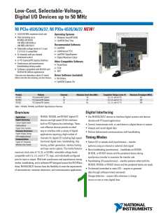
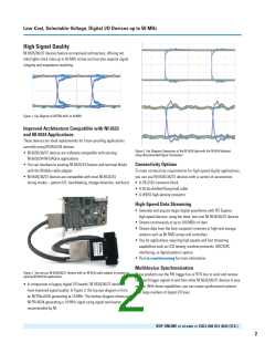
Low-Cost, Selectable-Voltage, Digital I/O Devices up to 50 MHz
Imported sample clock timebase/
frequency range
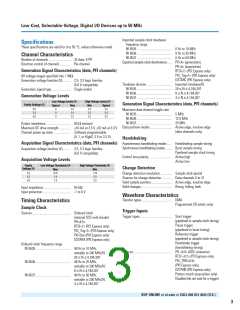
Specifications
These specifications are valid for 0 to 55 °C, unless otherwise noted.
NI 6535 .......................................... 0 Hz to 10 MHz
NI 6536 .......................................... 0 Hz to 25 MHz
NI 6537 .......................................... 0 Hz to 50 MHz
Exported sample clock destinations...... PFI<4> (generation)
PFI<5> (acquisition)
Channel Characteristics
Number of channels............................ 32 data, 6 PFI
Direction control of channels ............. Per-channel
Generation Signal Characteristics (data, PFI channels)
All voltage ranges specified into 1 MΩ
Generation voltage families (V).......... 2.5, 3.3 logic families
(5.0 V compatible)
RTSI<7> (PCI Express only)
PXI_Trig<7> (PXI Express only)
DSTARC (PXI Express only)
Timebase division ............................... Imported timebase/N;
NI 6535 ........................................... 20 ≤ N ≤ 4,194,307
NI 6536 ........................................... 8 ≤ N ≤ 4,194,307
NI 6537 ........................................... 4 ≤ N ≤ 4,194,307
Generation signal type........................ Single-ended
Generation Voltage Levels
Low Voltage Levels (V)
High Voltage Levels (V)
Generation Signal Characteristics (data, PFI channels)
Maximum data channel toggle rate
NI 6535 ........................................... 5 MHz
NI 6536 ........................................... 12.5 MHz
NI 6537 ........................................... 25 MHz
Data position modes........................... Active edge, inactive edge
(data channels only)
Family Settings (V)
Typical
Max
0.1
0.1
Min
2.4
3.2
Typical
2.5
3.3
2.5
3.3
5.0
0
0
0
0.1
3.2
3.3
Output impedance............................... 50 Ω nominal
Maximum DC drive strength............... 16 mA at 2.5 V, 32 mA at 3.3 V
Channel power-up state ..................... Software programmable
(0, 1, or HighZ; 2.5 or 3.3 V)
Handshaking
Asynchronous handshaking modes...... Handshaking sample timing
Synchronous handshaking modes........ Burst sample timing
Pipelined sample clock timing
Control line polarity ............................ Active high
Active low
Acquisition Signal Characteristics (data, PFI channels)
Acquisition voltage families (V).......... 2.5, 3.3 logic families
(5.0 V compatible)
Acquisition Voltage Levels
Family
Low Voltage Thresholds (V)
High Voltage Thresholds (V)
Change Detection
Settings (V)
Max
0.75
1.0
Min
1.75
2.3
2.5
3.3
5.0
Change detection resolution............... Sample clock period
Sources for change detection............. Data channels 0 to 31
Valid sample position.......................... Active edge, inactive edge
Valid changes...................................... Rising, falling, both
1.0
2.3
Input impedance ................................. 50 kΩ
Input protection................................... -1 to 6 V
Waveform Characteristics
Transfer types...................................... DMA
Programmed I/O (static only)
Timing Characteristics
Sample Clock
Trigger Inputs
Trigger types........................................ Start trigger
(pipelined or sample clock timing)
Pause trigger
Sources................................................ Onboard clock
(internal OSC with divider)
PFI<4:5>
RTSI<7> (PCI Express only)
PXI_Trig<7> (PXI Express only)
PXI-Star (PXI Express only)
DSTARA (PXI Express only)
(pipelined or burst timing)
Reference trigger
(pipelined or sample clock timing)
Handshake trigger
(handshaking timing)
Onboard clock frequency range
NI 6535 ........................................... 48 Hz to 10 MHz,
settable to 200 MHz/N;
20 ≤ N ≤ 4,194,307
NI 6536 ........................................... 48 Hz to 25 MHz,
settable to 200 MHz/N;
Sources................................................ PFI <0:5> (DDC connector)
RTSI <0:7> (PCI Express only)
PXI_TRIG<0:6>
(PXI Express only)
DSTARB (PXI Express only)
Pattern match (acquisition only)
Disabled (do not wait for a trigger)
8 ≤ N ≤ 4,194,307
NI 6537 ........................................... 48 Hz to 50 MHz,
settable to 200 MHz/N;
4 ≤ N ≤ 4,194,307
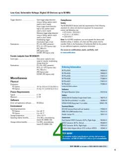
BUY ONLINE at ni.com or CALL 800 813 3693 (U.S.)
3

 NI [ National Instruments ]