Nexperia
PESD5V0U1BLD
Ultra low capacitance bidirectional ESD protection diode
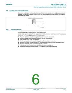
10. Application information
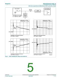
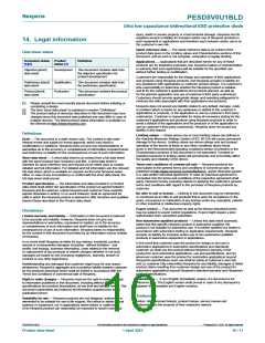
The device is designed for the protection of one bidirectional data line from surge pulses and ESD
damage. The device is suitable on lines where the signal polarities are both positive and negative
with respect to ground.
line to be protected
ESD protection diode
GND
aaa-002737
Fig. 7. Application diagram
Circuit board layout and protection device placement
Circuit board layout is critical for the suppression of ESD, Electrical Fast Transient (EFT) and surge
transients. The following guidelines are recommended:
1. Place the device as close to the input terminal or connector as possible.
2. Minimize the path length between the device and the protected line.
3. Keep parallel signal paths to a minimum.
4. Avoid running protected conductors in parallel with unprotected conductors.
5. Minimize all Printed-Circuit Board (PCB) conductive loops including power and ground loops.
6. Minimize the length of the transient return path to ground.
7. Avoid using shared transient return paths to a common ground point.
8. Use ground planes whenever possible. For multilayer PCBs, use ground vias.
©
PESD5V0U1BLD
All information provided in this document is subject to legal disclaimers.
Nexperia B.V. 2023. All rights reserved
Product data sheet
1 April 2023
6 / 11

 NEXPERIA [ Nexperia ]