Nexperia
74HC4050
Hex non-inverting HIGH-to-LOW level shifter
10. Dynamic characteristics
Table 7. Dynamic characteristics
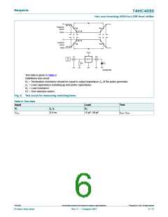
Voltages are referenced to GND (ground = 0 V); CL = 50 pF unless otherwise specified; for test circuit see Fig. 8.
Symbol Parameter
Conditions
25 °C
-40 °C to +85 °C -40 °C to +125 °C Unit
Min Typ Max
Min
Max
Min
Max
tpd
propagation nA to nY; see Fig. 7
[1]
delay
VCC = 2.0 V
-
-
-
-
25
9
85
17
-
-
-
-
-
105
21
-
-
-
-
-
130
26
-
ns
ns
ns
ns
VCC = 4.5 V
VCC = 5 V; CL = 15 pF
7
VCC = 6.0 V
Yn; see Fig. 7
VCC = 2.0 V
VCC = 4.5 V
VCC = 6.0 V
7
14
18
22
tt
transition
time
[2]
[3]
-
-
-
-
19
7
75
15
13
-
-
-
-
-
95
19
16
-
-
-
-
-
110
22
19
-
ns
ns
ns
pF
6
CPD
power
dissipation
capacitance
CL = 50 pF; f = 1 MHz;
VI = GND to VCC
14
[1] tpd is the same as tPLH and tPHL
.
[2] tt is the same as tTHL and tTLH
.
[3] CPD is used to determine the dynamic power dissipation (PD in μW).
PD = CPD x VCC 2 x fi x N + Σ(CL x VCC 2 x fo) where:
fi = input frequency in MHz;
fo = output frequency in MHz;
CL = output load capacitance in pF;
VCC = supply voltage in V;
N = number of inputs switching;
Σ(CL x VCC 2 x fo) = sum of outputs.
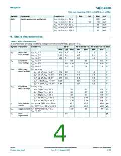
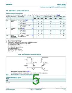
10.1. Waveforms and test circuit
V
I
V
V
M
nA input
GND
M
t
t
PHL
PLH
V
OH
90 %
V
V
nY output
M
M
10 %
V
OL
t
t
TLH
THL
aaa-006246
Measurement points are given in Table 8.
VOL and VOH are typical voltage output levels that occur with the output load.
Fig. 7. The input (nA) to output (nY) propagation delays
Table 8. Measurement points
Input
VM
Output
VM
0.5VCC
0.5VCC
©
74HC4050
All information provided in this document is subject to legal disclaimers.
Nexperia B.V. 2021. All rights reserved
Product data sheet
Rev. 5 — 3 August 2021
5 / 11

 NEXPERIA [ Nexperia ]