Nexperia
74HC4050
Hex non-inverting HIGH-to-LOW level shifter
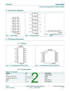
6. Functional description
Table 3. Function table
H = HIGH voltage level; L = LOW voltage level.
Input
nA
L
Output
nY
L
H
H
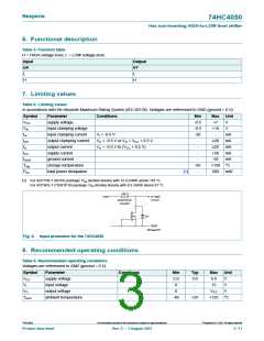
7. Limiting values
Table 4. Limiting values
In accordance with the Absolute Maximum Rating System (IEC 60134). Voltages are referenced to GND (ground = 0 V).
Symbol
VCC
VIK
Parameter
Conditions
Min
Max Unit
supply voltage
-0.5
+7
+16
-
V
input clamping voltage
input clamping current
output clamping current
output current
-0.5
V
IIK
VI < -0.5 V
-20
mA
mA
mA
mA
mA
IOK
VO < -0.5 V or VO > VCC + 0.5 V
VO = -0.5 V to (VCC + 0.5 V)
-
±20
±25
+50
-50
IO
-
ICC
supply current
-
-
IGND
Tstg
Ptot
ground current
storage temperature
total power dissipation
-65
-
+150 °C
[1]
500
mW
[1] For SOT109-1 (SO16) package: Ptot derates linearly with 12.4 mW/K above 110 °C.
For SOT403-1 (TSSOP16) package: Ptot derates linearly with 8.5 mW/K above 91 °C.
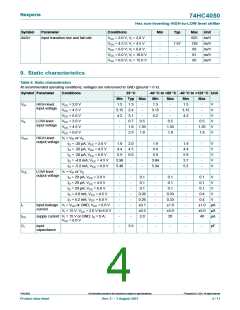
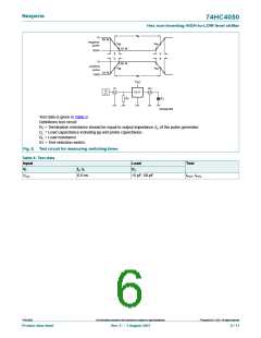
100 Ω
input
to logic
circuit
polysilicon
resistor
D1
GND
001aan375
Fig. 6. Input protection for the 74HC4050
8. Recommended operating conditions
Table 5. Recommended operating conditions
Voltages are referenced to GND (ground = 0 V)
Symbol
VCC
VI
Parameter
Conditions
Min
2.0
0
Typ
Max
6.0
Unit
V
supply voltage
input voltage
5.0
-
-
15
V
VO
output voltage
ambient temperature
0
VCC
V
Tamb
-40
+25
+125 °C
©
74HC4050
All information provided in this document is subject to legal disclaimers.
Nexperia B.V. 2021. All rights reserved
Product data sheet
Rev. 5 — 3 August 2021
3 / 11

 NEXPERIA [ Nexperia ]