µPD75304B,75306B,75308B
11. ELECTRICAL SPECIFICATIONS
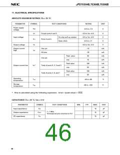
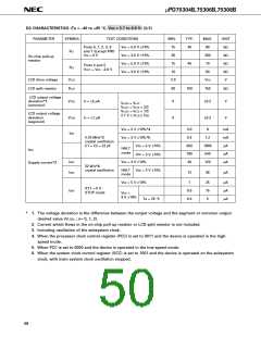
ABSOLUTE MAXIMUM RATINGS (Ta = 25 °C)
PARAMETER
SYMBOL
TEST CONDITIONS
RATING
UNIT
V
Power supply
voltage
VDD
VI1
–0.3 to +7.0
Except ports 4 and 5
–0.3 to VDD +0.3
V
Input voltage
On-chip pull-up resistor
Open–drain
–0.3 to VDD +0.3
V
V12
VO
IOH
Ports 4 and 5
–0.3 to +11
V
Output voltage
–0.3 to VDD +0.3
V
Output current
high
One pin
All pins
–15
–30
30
mA
mA
mA
mA
mA
mA
mA
mA
Peak value
rms
One pin
15
Peak value
100
60
Output current low
IOL*
Total of ports 0, 2, 3 and 5
Total of ports 4, 6, and 7
rms
Peak value
rms
100
60
Operating
temperature
–40 to +85
°C
°C
Topt
Tstg
Storage
temperature
–65 to +150
*
Rms is calculated using the following expression: [rms] = [peak value] × √duty
CAPACITANCE (Ta = 25 °C, VDD = 0 V)
PARAMETER
Input capacitance
Output capacitance
I/O capacitance
SYMBOL
CIN
TEST CONDITIONS
MIN.
TYP.
MAX.
UNIT
pF
15
15
15
f = 1 MHz
Unmeasured pins returned to 0 V.
COUT
pF
CIO
pF
46

 NEC [ NEC ]