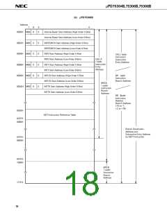
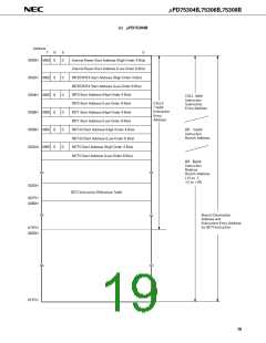
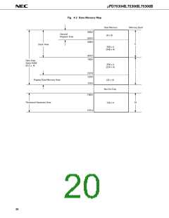
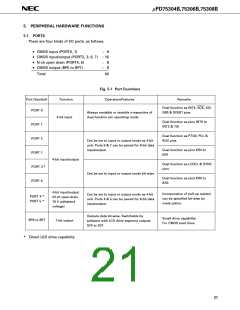
µPD75304B,75306B,75308B
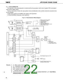
5.2 CLOCK GENERATOR
The operation of the clock generator is determined by the processor clock control register (PCC) and system
clock control register (SCC).
There are two kinds of clock, the main system clock and subsystem clock, and the instruction execution time
can be changed.
• 0.95 µs/1.91 µs/15.3 µs (4.19 MHz main system clock operation)
• 122 µs (32.768 kHz subsystem clock operation)
Fig. 5-1 Clock Generator Block Diagram
• Basic Interval Timer (BT)
• Timer/Event Counter
• Serial Interface
XT1
V
DD
Subsystem
Clock Oscil-
lation Circuit
LCD Controller/
Driver
Watch Timer
f
XT
• Watch Timer
• LCD Controller/Driver
• INT0 Noise Elimination Circuit
• Clock Output Circuit
XT2
X1
V
DD
Main System
Clock Oscil-
lation Circuit
fX
1/8 to 1/4096
Frequency Divider
X2
1/2 1/16
Oscil-
lation
Stop
WM. 3
SCC
Frequency
Divider
SCC3
Φ
1/4
SCC0
PCC
• CPU
• INT0 Noise
Elimination Circuit
• Clock Output Circuit
PCC0
PCC1
PCC2
PCC3
4
HALT F/F
S
HALT *
STOP *
R
Q
PCC2,
PCC3
Clear
Wait Release Signal from BT
RESET Signal
STOP F/F
Q
S
R
Standby Release Signal from
Interrupt Control Circuit
Remarks 1. fX = Main system clock frequency
2. fXT = Subsystem clock frequency
3. PCC: Processor clock control register
4. SCC: System clock control register
5. * indicates instruction execution.
6. One Φ clock cycle (tCY) is one machine cycle. See "AC CHARACTERISTICS" in 11. "ELECTRICAL
SPECIFICATIONS" for details of tCY.
★
22

 NEC [ NEC ]