µPD75216A
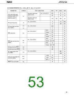
DATA MEMORY STOP MODE LOW POWER SUPPLY VOLTAGE DATA RETENTION CHARACTERISTICS (Ta = –40
to +85 °C)
PARAMETER
SYMBOL
TEST CONDITIONS
MIN.
2.0
TYP.
0.1
MAX.
6.0
UNIT
V
Data retention power
supply voltage
VDDDR
Data retention power
IDDDR
tSREL
VDDDR = 2.0V
10
µA
µs
supply current *1
Release signal set time
0
Release by RESET
217/fX
ms
ms
Oscillation stabilization
tWAIT
wait time *2
Release by interrupt request
*3
*
1. Current to the on-chip pull-down resistor and power-on reset circuit (mask option) is not included.
2. Oscillation stabilization wait time is time to stop CPU operation to prevent unstable operation upon oscillation
start.
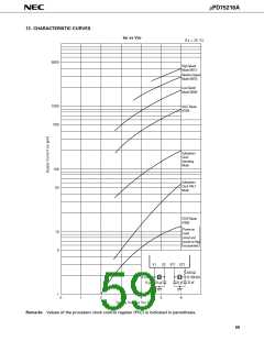
3. According to the setting of the basic interval timer mode register (BTM) (see below).
BTM3
—
BTM2
BTM1
BTM0
Wait Time (Values at fXX = 4.19 MHz in parentheses)
220/fXX (approx. 250 ms)
0
0
1
1
0
1
0
1
0
1
1
1
—
217/fXX (approx. 31.3 ms)
—
215/fXX (approx. 7.82 ms)
—
213/fXX (approx. 1.95 ms)
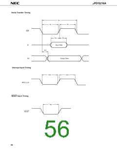
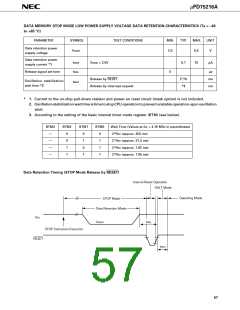
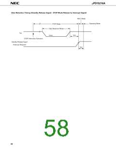
Data Retention Timing (STOP Mode Release by RESET)
Internal Reset Operation
HALT Mode
Operating Mode
STOP Mode
Data Retention Mode
VDD
tSREL
VDDDR
STOP Instruction Execution
RESET
t
WAIT
57

 NEC [ NEC ]