CONTENTS
CHAPTER 1 OVERVIEW OF EACH PRODUCT..................................................................................10
1.1 Outline ...........................................................................................................................................10
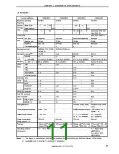
1.2 Features.........................................................................................................................................11
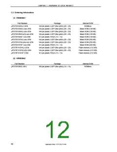
1.3 Ordering Information....................................................................................................................12
1.4 Pin Configuration..........................................................................................................................14
1.5 Internal Block Diagram ................................................................................................................25
CHAPTER 2 OVERVIEW OF PCI HOST BRIDGE MACRO..............................................................29
2.1 Outline ...........................................................................................................................................29
2.2 Features.........................................................................................................................................30
CHAPTER 3 SPECIFICATIONS OF PCI HOST BRIDGE MACRO...................................................31
3.1 Internal Blocks of PCI Host Bridge Macro .................................................................................31
3.2 Relationship Between Internal Blocks and Signals..................................................................32
3.3 Pin Functions................................................................................................................................33
3.3.1 External bus slave interface pins .......................................................................................................33
3.3.2 SDRAM bus interface pins.................................................................................................................33
3.3.3 PCI bus interface pins........................................................................................................................34
3.4 Registers .......................................................................................................................................35
3.4.1 PCI_CONFIG_DATA register.............................................................................................................35
3.4.2 PCI_CONFIG_ADD register...............................................................................................................36
3.4.3 PCI_CONTROL register.....................................................................................................................37
3.4.4 PCI_IO_BASE register.......................................................................................................................38
3.4.5 PCI_MEM_BASE register ..................................................................................................................38
3.4.6 PCI_INT_CTL register........................................................................................................................39
3.4.7 PCI_ERR_ADD register.....................................................................................................................40
3.4.8 SYSTEM_MEM_BASE register .........................................................................................................41
3.4.9 SYSTEM_MEM_RANGE register ......................................................................................................41
3.4.10 SDRAM_CTL register ........................................................................................................................42
3.5 Address Map .................................................................................................................................44
3.6 Initializing PCI Host Bridge Macro..............................................................................................45
3.7 Bus Width of External Bus Interface ..........................................................................................46
3.8 Timing............................................................................................................................................47
3.8.1 External bus interface timing..............................................................................................................47
3.8.2 PCI bus interface timing.....................................................................................................................50
CHAPTER 4 CONFIGURATION EXAMPLES OF FPGA INTEGRATION..........................................57
4.1 Conditions for Configuration Examples of FPGA Integration .................................................57
4.2 Points to Remember When Creating Top Layer of FPGA ........................................................57
4.3 Reference Diagram for FPGA Top Connection .........................................................................58
4.4 FPGA Top Pin Functions .............................................................................................................59
4.4.1 CPU bus slave interface pins.............................................................................................................59
4.4.2 SDRAM bus interface pins.................................................................................................................59
4.4.3 PCI bus interface pins........................................................................................................................60
4.5 FPGA Top Pin Configuration.......................................................................................................61
8
Application Note U17121EJ1V1AN

 NEC [ NEC ]