CHAPTER 1 INTRODUCTION
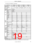
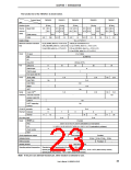
The function list of the V850ES/Kx1+ is shown below.
Product Name
Number of pins
V850ES/KE1+
64 pins
V850ES/KF1+
V850ES/KG1+
V850ES/KJ1+
144 pins
80 pins
256
−
100 pins
Internal
memory
(KB)
Mask ROM
Flash memory
RAM
128
−
−
128
6
−
−
128
6
256
−
−
−
−
−
128
256
256
128
6
256
16
4
12
16
Supply voltage
2.7 to 5.5 V
Minimum instruction execution time
50 ns @20 MHz
Clock
X1 input
2 to 10 MHz
Subclock
32.768 kHz
Ring-OSC
CMOS input
CMOS I/O
N-ch open-drain I/O
16-bit (TMP)
16-bit (TM0)
8-bit (TM5)
8-bit (TMH)
Interval timer
Watch
240 kHz (TYP.)
Port
8
8
8
16
112
6
43
59
76
2
2
4
Timer
1 ch
1 ch
2 ch
2 ch
1 ch
1 ch
1 ch
1 ch
6 bits × 1 ch
2 ch
−
1 ch
2 ch
2 ch
2 ch
1 ch
1 ch
1 ch
1 ch
1 ch
4 ch
2 ch
2 ch
1 ch
1 ch
1 ch
1 ch
1 ch
6 ch
2 ch
2 ch
1 ch
1 ch
WDT1
1 ch
WDT2
1 ch
RTO
6 bits × 1 ch
2 ch
6 bits × 1 ch
2 ch
6 bits × 2 ch
3 ch
Serial
CSI
interface
Automatic transmit/receive
3-wire CSI
1 ch
2 ch
2 ch
UART
1 ch
1 ch
2 ch
2 ch
UART supporting LIN-bus
I2CNote
1 ch
1 ch
1 ch
1 ch
1 ch
1 ch
1 ch
2 ch
External
bus
Address space
Address bus
Mode
−
128 KB
3 MB
15 MB
24 bits
−
16 bits
22 bits
−
Multiplex only
Multiplex/separate
DMA controller
10-bit A/D converter
8-bit D/A converter
Interrupt External
Internal
−
−
4 ch
8 ch
2 ch
9
4 ch
16 ch
2 ch
9
8 ch
8 ch
−
−
9
9
27
30
8 ch
42
48
Key return input
8 ch
8 ch
8 ch
Reset
RESET pin
Provided
POC
2.7 V or less fixed
LVI
3.1 V/3.3 V 0.15 V or 3.5 V/3.7 V/3.9 V/4.1 V/4.3 V 0.2 V (selectable by software)
Clock monitor
WDT1
WDT2
Provided (monitor by Ring-OSC)
Provided
Provided
ROM correction
4
None
Regulator
None
Provided
Standby function
Operating ambient temperature
HALT/IDLE/STOP/sub-IDLE mode
= −40 to +85°C
TA
Note Only in products with an I2C bus (Y products). For the product name, refer to each user’s manual.
19
User’s Manual U16890EJ1V0UD

 NEC [ NEC ]