CHAPTER 3 CPU FUNCTIONS
3.3 Operation Modes
The V850ES/KF1, V850ES/KG1, and V850ES/KJ1 have the following operating modes.
(1) Normal operating mode
After the system has been released from the reset state, the pins related to the bus interface are set to the port
mode, execution branches to the reset entry address of the internal ROM, and instruction processing is
started. An external device can be connected to the external memory area by setting the PMCDH, PMCDL,
PMCCM, PMCCS, and PMCCT registers to the control mode via software.
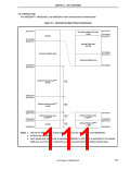
(2) Flash memory programming mode
µPD70F3210, 70F3210Y: V850ES/KF1
µPD70F3214, 70F3214Y: V850ES/KG1
µPD70F3217, 70F3217Y: V850ES/KJ1
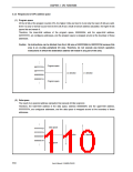
The internal flash memory can be written or erased when 10 V 0.3 V is applied to the VPP pin.
VPP
Operating Mode
Normal operation mode
0
10 0.3 V
VDD
Flash memory programming mode
Setting prohibited
User’s Manual U15862EJ3V0UD
107

 NEC [ NEC ]