µPC2710TB
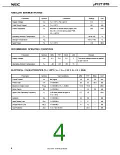
ABSOLUTE MAXIMUM RATINGS
Parameter
Supply Voltage
Symbol
Conditions
TA = +25°C, Pin 4 and 6
Ratings
Unit
V
VCC
ICC
5.8
60
Total Circuit Current
Power Dissipation
TA = +25°C
mA
mW
PD
Mounted on double-sided copper clad
50 × 50 × 1.6 mm epoxy glass PWB
(TA = +85°C)
200
Operating Ambient Temperature
Storage Temperature
Input Power
TA
Tstg
Pin
−40 to +85
−55 to +150
+10
°C
°C
TA = +25°C
dBm
RECOMMENDED OPERATING CONDITIONS
Parameter
Supply Voltage
Symbol
VCC
MIN.
4.5
TYP.
5.0
MAX.
5.5
Unit
V
Remark
The same voltage should be applied
to pin 4 and 6.
Operating Ambient Temperature
TA
−40
+25
+85
°C
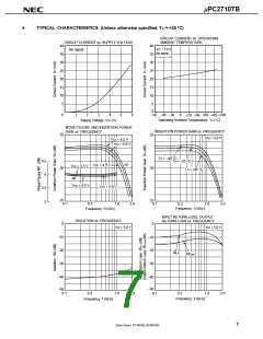
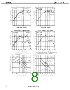
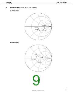
ELECTRICAL CHARACTERISTICS (TA = +25°C, VCC = Vout = 5.0 V, ZS = ZL = 50 Ω)
Parameter
Circuit Current
Symbol
ICC
Test Conditions
MIN.
16
TYP.
22
MAX.
29
Unit
mA
dB
No Signal
Power Gain
GP
f = 500 MHz
30
33
36.5
–
Maximum Output Level
Noise Figure
PO(sat)
NF
f = 500 MHz, Pin = –8 dBm
f = 500 MHz
+11.0
–
+13.5
3.5
dBm
dB
5.0
–
Upper Limit Operating Frequency
fu
3 dB down below flat gain at
f = 0.1 GHz
0.7
1.0
GHz
Isolation
ISL
RLin
RLout
∆GP
f = 500 MHz
34
3
39
6
–
–
–
–
dB
dB
dB
dB
Input Return Loss
Output Return Loss
Gain Flatness
f = 500 MHz
f = 500 MHz
9
12
f = 0.1 to 0.6 GHz
–
±0.8
4
Data Sheet P13443EJ2V0DS00

 NEC [ NEC ]