µPC2710TB
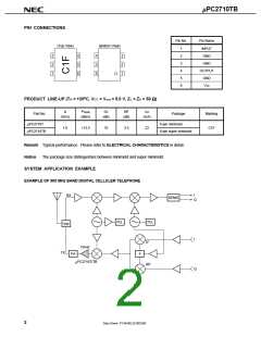
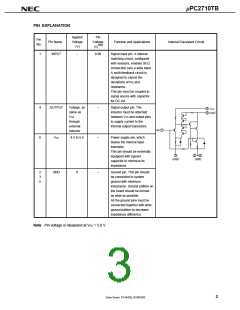
PIN EXPLANATION
Applied
Voltage
(V)
Pin
Pin
Voltage
(V)Note
Pin Name
No.
Function and Applications
Internal Equivalent Circuit
1
INPUT
–
0.90
Signal input pin. A internal
matching circuit, configured
with resistors, enables 50 Ω
connection over a wide band.
A multi-feedback circuit is
designed to cancel the
deviations of hFE and
resistance.
This pin must be coupled to
signal source with capacitor
for DC cut.
4
6
OUTPUT
Voltage as
same as
VCC
–
–
Signal output pin. The
6
4
V
CC
inductor must be attached
between VCC and output pins
to supply current to the
internal output transistors.
OUT
through
external
inductor
1
IN
VCC
4.5 to 5.5
Power supply pin, which
biases the internal input
transistor.
This pin should be externally
equipped with bypass
capacitor to minimize its
impedance.
3
GND
2
GND
5
2
3
5
GND
0
–
Ground pin. This pin should
be connected to system
ground with minimum
inductance. Ground pattern on
the board should be formed
as wide as possible.
All the ground pins must be
connected together with wide
ground pattern to decrease
impedance difference.
Note Pin voltage is measured at VCC = 5.0 V
3
Data Sheet P13443EJ2V0DS00

 NEC [ NEC ]