CHAPTER 4 PORT FUNCTIONS
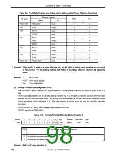
Table 4-3. Port Mode Register and Output Latch Settings When Using Alternate Functions
Alternate Function
PMxx
Pxx
Pin Name
Name
KR0 to KR3
I/O
P00 to P03
P26
Input
1
0
1
1
1
0
1
1
0
1
0
1
x
0
x
x
x
0
x
x
0
x
0
x
TO90
Output
Input
P30
INTP0
CPT90
INTP1
TO50
Input
P31
Input
Output
Input
TMI60
INTP2
TO60
P32
Input
Output
Input
P33
INTP3
TO61
Output
Input
P60 to P65
ANI0 to ANI5
Caution When port 2 is used as a serial interface pin, the I/O latch or output latch must be set according
to its function. For the setting method, see Table 12-2 Settings of Serial Interface 20 Operating
Mode.
Remark x:
PMxx: Port mode register
Pxx: Port output latch
don’t care
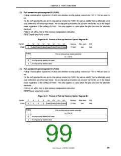
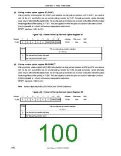
(2) Pull-up resistor option register 0 (PU0)
Pull-up resistor option register 0 (PU0) sets whether on-chip pull-up registers are used on ports 0 and 1 or
not.
On the port specified to use an on-chip pull-up resistor by PU0, the pull-up resistor can be internally used
only for the bits set in the input mode. No on-chip pull-up resistors can be used for the bits set in the output
mode regardless of the setting of PU0. This also applies to cases when the pins are used for alternate
functions.
PU0 is set with a 1-bit or 8-bit memory manipulation instruction.
RESET input sets PU0 to 00H.
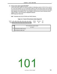
Figure 4-19. Format of Pull-Up Resistor Option Register 0
Symbol
PU0
7
0
6
0
5
0
4
0
3
0
2
0
<1> <0>
Address
FFF7H
After reset
00H
R/W
R/W
PU01 PU00
PU0m
Pm on-chip pull-up resistor selection
(m = 0, 1)
0
1
On-chip pull-up resistor not used
On-chip pull-up resistor used
Caution Bits 2 to 7 must be set to 0.
98
User’s Manual U15075EJ1V0UM00

 NEC [ NEC ]