CHAPTER 1 GENERAL
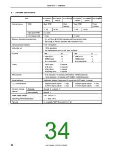
1.7 Overview of Functions
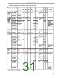
Item
µPD789425, µPD789426, µPD78F9436 µPD789445, µPD789446, µPD78F9456
789435
789436
789455
789456
Internal memory
ROM
Mask ROM
Flash
Mask ROM
Flash
memory
memory
12 KB
16 KB
12 KB
16 KB
High-speed RAM
LCD display RAM
512 bytes
5 bytes
15 bytes
Minimum instruction execution time
• 0.4 µs/1.6 µs (@ 5.0 MHz operation with main system clock)
• 122 µs (@ 32.768 kHz operation with subsystem clock)
General-purpose registers
Instruction set
8 bits × 8 registers
• 16-bit operations
• Bit manipulations (such as set, reset, and test)
I/O ports
Total:
40
Total:
30
• CMOS I/O:
30
6
• CMOS I/O:
20
6
• CMOS input:
• N-ch open-drain:
• CMOS input:
• N-ch open-drain:
4
4
Timers
• 16-bit timer:
• 8-bit timer:
1 channel
2 channels
1 channel
1 channel
• Watch timer:
• Watchdog timer:
A/D converter
• 8-bit resolution × 6 channels (µPD789426, 789446 Subseries)
• 10-bit resolution × 6 channels (µPD789436, 789456 Subseries)
Serial interfaces
Switchable between 3-wire serial I/O mode and UART mode: 1 channel
LCD controller/driver
• Segment signal outputs:
• Common signal outputs:
5 max.
4 max.
• Segment signal outputs: 15 max.
• Common signal outputs: 4 max.
Maskable
Internal: 9, external: 5
Internal: 1
Vectored interrupt
sources
Non-maskable
Power supply voltage
VDD = 1.8 to 5.5 V
TA = −40 to +85°C
Operating ambient temperature
Package
64-pin plastic TQFP (fine pitch) (12 × 12)
34
User’s Manual U15075EJ1V0UM00

 NEC [ NEC ]