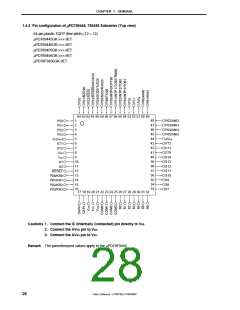
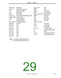
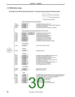
CHAPTER 1 GENERAL
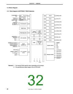
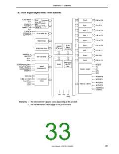
1.6 Block Diagram
1.6.1 Block diagram of µPD789426, 789436 Subseries
TO50/TMI60/
P31
Cascaded
16-bit
timer/
event
counter
Port 0
Port 1
Port 2
Port 3
Port 5
Port 6
Port 7
Port 8
Port 9
8-bit
timer 50
P00 to P03
TO60/P32
TO61/P33
TMI60/TO50/
8-bit
P10, P11
timer/event
counter 60
P31
P20 to P26
P30 to P33
P50 to P53
P60 to P65
P70 to P72
P80, P81
TO90/P26
CPT90/P30
BZO90/P21
16-bit timer 90
Watch timer
ROM
(flash
memory)
78K/0S
CPU core
Watchdog timer
ANI0/P60 to
ANI5/P65
AVDD
A/D converter
AVSS
P90 to P97
RAM space
for LCD
data
RAM
RESET
X1
SCK20/ASCK20/P23
SO20/TxD20/P24
Serial
Iinterface 20
SI20/RxD20/P25
SS20/P22
System control
X2
XT1
XT2
S0 to S4
INTP0/P30
INTP1/P31
COM0 to COM3
LCD controller
driver
V
LC0 to VLC2
INTP2/P32
INTP3/P33
CAPH
CAPL
Interrupt control
KR0/P00 to
KR3/P03
VDD
VSS
IC
(VPP
)
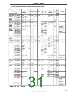
Remarks 1. The internal ROM capacity varies depending on the product.
2. The parenthesized values apply to the µPD78F9436.
32
User’s Manual U15075EJ1V0UM00

 NEC [ NEC ]