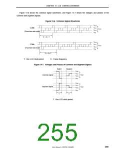
CHAPTER 13 LCD CONTROLLER/DRIVER
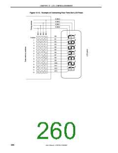
13.7.2 Four-time slot display example
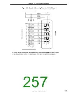
Figure 13-12 shows how the 7-digit LCD panel having the display pattern shown in Figure 13-11 is connected to
the segment signals (S0 to S14) and the common signals (COM0 to COM3) of the µPD789446 or µPD789456
Subseries chip. This example displays data “123456.7” in the LCD panel. The contents of the display data memory
(addresses FA00H to FA0EH) correspond to this display.
The following description focuses on numeral “6.” ( ) displayed in the seventh digit. To display “6.” in the LCD
panel, it is necessary to apply the select or deselect voltage to the S2 and S3 pins according to Table 13-7 at the
timing of the common signals COM0 to COM3.
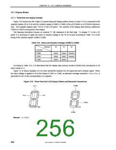
Table 13-7. Select and Deselect Voltages (COM0 to COM3)
Segment
S2
S3
Common
COM0
COM1
COM2
COM3
Select
Deselect
Select
Select
Select
Select
Select
Select
According to Table 13-7, it is determined that the display data memory location (FA02H) that corresponds to S2
must contain 1101.
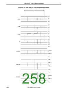
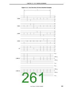
Figure 13-13 shows examples of LCD drive waveforms between the S2 signal and the COM0 or COM1 signal
(the waveforms for COM2 and COM3 have been left out from the drawing). When the select voltage is applied to S2
at the timing of COM0, an alternate rectangle waveform, +VLCD/–VLCD, is generated to turn on the corresponding LCD
segment.
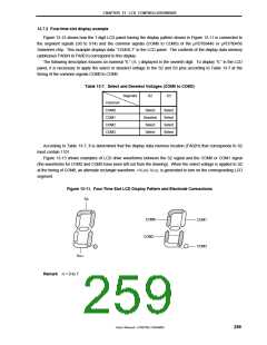
Figure 13-11. Four-Time Slot LCD Display Pattern and Electrode Connections
S2n
COM0
COM2
COM1
COM3
S2n+1
Remark n = 0 to 7
User’s Manual U15075EJ1V0UM00
259

 NEC [ NEC ]