CHAPTER 5 CLOCK GENERATOR
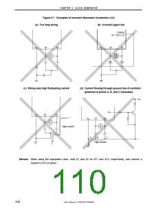
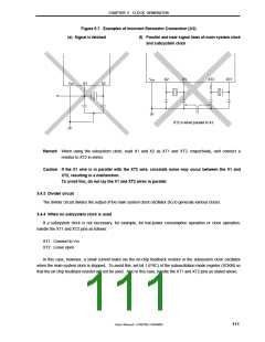
Figure 5-7. Examples of Incorrect Resonator Connection (2/2)
(e) Signal is fetched
(f) Parallel and near signal lines of main system clock
and subsystem clock
X2
X1
XT2
XT1
VSS
X1
X2
VSS
XT2 is wired parallel to X1.
Remark When using the subsystem clock, read X1 and X2 as XT1 and XT2, respectively, and connect a
resistor to XT2 in series.
Caution If the X1 wire is in parallel with the XT2 wire, crosstalk noise may occur between the X1 and
XT2, resulting in a malfunction.
To avoid this, do not lay the X1 and XT2 wires in parallel.
5.4.3 Divider circuit
The divider circuit divides the output of the main system clock oscillator (fX) to generate various clocks.
5.4.4 When no subsystem clock is used
If a subsystem clock is not necessary, for example, for low-power consumption operation or clock operation,
handle the XT1 and XT2 pins as follows:
XT1: Connect to VSS
XT2: Leave open
In this case, however, a small current leaks via the on-chip feedback resistor in the subsystem clock oscillator
when the main system clock is stopped. To avoid this, set bit 1 (FRC) of the suboscillation mode register (SCKM) so
that the on-chip feedback resistor will not be used. Also in this case, handle the XT1 and XT2 pins as stated above.
User’s Manual U15075EJ1V0UM00
111

 NEC [ NEC ]