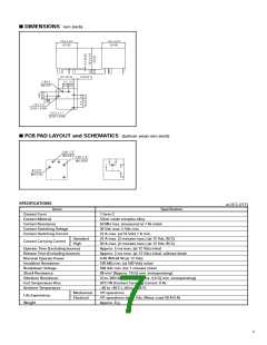
■ DIMENSIONS m m (inch)
[H Bridge Type]
[Separate (T) Type]
23.8 ± 0.5
16.2 ± 0.5
23.8 ± 0.5
16.2 ± 0.5
(0.94)
(0.64)
(0.94)
(0.64)
10.1
8.0 (0.31)
(0.4)
10.1
8.0 (0.31)
(0.4)
4-0.5 × 1.1 (0.02 × 0.04)
2-0.5 × 1.1 (0.02 × 0.04)
3.5
3.5
(0.14)
(0.14)
(0.14) 3.5
(0.14) 3.5
2-1.3 × 1.3
(0.05 × 0.05)
2-1.3 × 1.3
(0.05 × 0.05)
(0.31) 8.0
(0.31) 8.0
(0.4) 10.1
(0.4) 10.1
φ
φ
4- 0.6
4- 0.6
φ
(
φ
(
0.02)
0.02)
■ PCB PAD LAYOUT and SCHEMATICS (bottom view) m m (inch)
[H Bridge Type]
[Separate (T) Type]
+0.1
+0.1
φ
φ
φ
4- 1.5 –0
4- 1.1 –0
+0.1
+0.1
φ
φ
φ
φ
4- 1.1 –0
2- 1.5 –0
φ
( 0.059)
( 0.043)
( 0.043)
( 0.059)
2
3
9
2
3
1
4
1
4
10
6
8
8
5
6
7
6
7
+0.1
φ
φ
2- 1.9 –0
+0.1
φ
φ
2- 1.9 –0
( 0.075)
(Side A)
(Side B)
(Unit A)
(Unit B)
( 0.075)
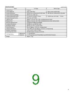
SPECIFICATIONS
at 25˚C (77˚F)
Item s
Specification
Contact Form
1 form C × 2 [H Bridge Type & Separate Type]
Silver oxide com plex alloy (Special types available)
50 m Ω m ax. (m easured at 7 A) initial
Contact Material
Contact Resistance
Contact Switching Voltage
Contact Switching Current
30 Vdc m ax.
5 Vdc m in.
1 A m in.
25 A m ax. (at 16 Vdc)
Standard
20 A m ax. (2 m inutes m ax.) (at 12 Vdc, 85˚C)
25 A m ax. (2 m inutes m ax.) (at 12 Vdc, 85˚C)
Approx. 5 m s m ax. (at 12 Vdc, excluding bounce) initial
Contact Carrying Current
High
Operate Tim e
Release Tim e
Approx. 2 m s m ax. (at 12 Vdc, excluding bounce) initial, without diode
0.48 W/0.64 W (at 12 Vdc)
Nom inal Operate Power
Insulation Resistance
Breakdown Voltage
Shock Resistance
100 MΩ m in. (at 500 Vdc) initial
500 Vdc m in. (for 1 m inute) initial
98 m /s2 [Approx. 10 G] m in. (m isoperating)
10 to 300 Hz, 43 m /s2 [Approx. 4.4 G] m in. (m isoperating)
–40˚C to +85˚C (–40˚ F to +185˚F)
Vibration Resistance
Am bient Tem perature
Coil Tem perature Rise
50˚C/W (contact carrying current 0 A)
1 x 10⁶ operations
1 x 10⁵ operations (at 14 Vdc, Motor Load 20 A/3 A)
Mechanical
Electrical
Life Expectancy
Weight
Approx. 15 gr.
5

 NEC [ NEC ]