2SK3326
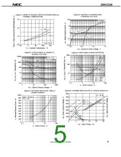
ELECTRICAL CHARACTERISTICS (TA = 25 °C)
CHARACTERISTICS
Drain Leakage Current
SYMBOL
IDSS
TEST CONDITIONS
VDS = 500 V, VGS = 0 V
MIN. TYP. MAX. UNIT
100
±100
3.5
µA
nA
V
Gate to Source Leakage Current
Gate to Source Cut-off Voltage
Forward Transfer Admittance
Drain to Source On-state Resistance
Input Capacitance
IGSS
VGS = ±30 V, VDS = 0 V
VDS = 10 V, ID = 1 mA
VGS(off)
| yfs |
RDS(on)
Ciss
2.5
2.0
VDS = 10 V, ID = 5.0 A
VGS = 10 V, ID = 5.0 A
4.0
0.68
1200
190
10
S
0.85
Ω
VDS = 10 V, VGS = 0 V, f = 1 MHz
pF
pF
pF
ns
ns
ns
ns
nC
nC
nC
V
Output Capacitance
Coss
Crss
Reverse Transfer Capacitance
Turn-on Delay Time
td(on)
tr
td(off)
tf
VDD = 150 V, ID = 5.0 A, VGS(on) = 10 V,
21
RG = 10 Ω, RL = 60 Ω
Rise Time
11
Turn-off Delay Time
40
Fall Time
9.5
22
Total Gate Charge
QG
VDD = 400 V, VGS = 10 V, ID = 10 A
Gate to Source Charge
Gate to Drain Charge
Body Diode Forward Voltage
QGS
QGD
VF(S-D)
6.5
7.5
1.0
IF = 10 A, VGS = 0 V
Reverse Recovery Time
Reverse Recovery Charge
trr
IF = 10 A, VGS = 0 V, di/dt = 50 A/µs
0.5
2.6
µs
Qrr
µC
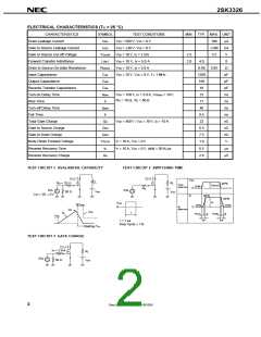
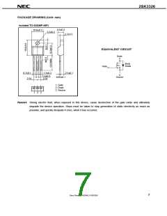
TEST CIRCUIT 1 AVALANCHE CAPABILITY
TEST CIRCUIT 2 SWITCHING TIME
D.U.T.
L
D.U.T.
V
GS
R
L
RG
= 25 Ω
90%
90%
V
GS
Wave Form
V
GS(on)
10%
0
R
G
PG.
PG.
50 Ω
V
DD
VDD
V
GS = 20→0V
I
D
90%
I
D
V
0
GS
BVDSS
10%
10%
I
D
0
Wave Form
I
AS
VDS
τ
I
D
t
d(on)
t
r
t
d(off)
tf
VDD
t
on
toff
τ = 1 µs
Duty Cycle ≤ 1 %
Starting Tch
TEST CIRCUIT 3 GATE CHARGE
D.U.T.
= 2 mA
I
G
RL
PG.
50 Ω
V
DD
2
Data Sheet D14204EJ1V0DS00

 NEC [ NEC ]