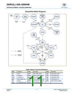
DDR3(L) 4Gb SDRAM
NT5CB(C)512M8DN / NT5CB(C)256M16DP
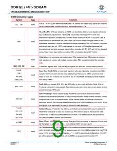
Symbol
Type
Function
Active Low Asynchronous Reset: Reset is active when REET is LOW, and inactive when
REET is HIGH. REET must be HIGH during normal operation. REET is a CMOS rail to rail
signal with DC high and low at 80% and 20% of VDD, i.e. 1.20V for DC high and 0.30V.
Data Inputs/Output: Bi-directional data bus. DQ0 is the prime DQ in a low byte lane of
x4/x8/x16 configuration and DQ8 is the prime DQ in a high byte lane of x16 configuration for write
leveling.
Input
REET
DQ
Input/output
Input/output
Data Strobe: output with read data, input with write data. Edge aligned with read data, centered
with write data. The data strobes DQS, DQSL, DQSU are paired with differential signals ,
L, U, respectively, to provide differential pair signaling to the system during both reads
and writes. DDR3 SDRAM supports differential data strobe only and does not support
single-ended.
For x8,
DQS, ()
For x16,
DQSL,(L),
DQSU,(U)
Termination Data Strobe: TDQS/T is applicable for X8 DRAMs only. When enabled via
Mode Register A11=1 in MR1, DRAM will enable the same termination resistance function on
TDQS/T that is applied to DQS/. When disabled via mode register A11=0 in MR1,
DM/T will provide the data mask function and T is not used. x16 DRAMs must disable the
TDQS function via mode register A11=0 in MR1.
For x8,
Output
TDQS, (T)
NC
-
No Connect: No internal electrical connection is present.
VDDQ
VDD
Supply
Supply
Supply
Supply
Supply
Supply
Supply
DQ Power Supply: 1.35V -0.067V/+0.1V or 1.5V ± 0.075V
Power Supply: 1.35V -0.067V/+0.1V or 1.5V ± 0.075V
DQ Ground
VSSQ
VSS
Ground
VREFCA
VREFDQ
ZQ
Reference voltage for CA
Reference voltage for DQ
Reference pin for ZQ calibration.
Notes:
1. Input only pins (BA0-BA2, A0-A15, RA, A, WE, , CKE, ODT, and REET) do not supply termination.
2. The signal may show up in a different symbol but it indicates the same thing. e.g., /CK = CK# = = CKb, /DQS = DQS# =
= DQSb, /CS = CS# = = CSb.
Version 2.3
02/2017
10
Nanya Technology Cooperation ©
All Rights Reserved.

 NANYA [ Nanya Technology Corporation. ]