NTC Proprietary
Level: Property
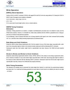
DDR3(L)-2Gb SDRAM
NT5CB(C)256M8JQ/NT5CB(C)128M16JR
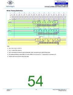
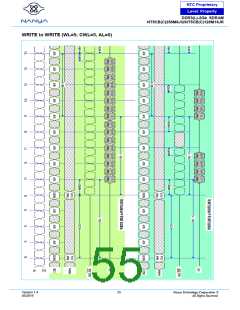
Write Timing Definition
T0
T1
T2
T3
T4
T5
T6
T7
T8
T9
Tn
CK
CK
CMD
Write
NOP
NOP
NOP
NOP
NOP
NOP
tDSH
NOP
tDSH
NOP
NOP
NOP
Bank
Col n
Address
tWPST(min)
tDSH
tDQSS tDSH
tDSS
tWPRE(min)
DQS, DQS
(tDQSS min)
tDQSL(min)
tDSS
tDQSH
tDSS
Din
tDQSH tDQSL tDQSH
tDSS
Din
Din
n
Din
n +1
Din
n +3
Din
n +5
Din
Din
DQ
n +2
n +4
n +6
n +7
tDSS
WL = AL + CWL
tWPST(min)
tDSH
tDSH
tDSH
tDSH
tDSS
tWPRE(min)
DQS, DQS
(tDQSS nominal)
tDQSL(min)
tDSS
tDQSH
tDSS
tDQSH tDQSL tDQSH
tDSS
Din
n
Din
n +1
Din
n +2
Din
n +3
Din
n +4
Din
n +5
Din
n +6
Din
DQ
n +7
tDSS
tDSH
tDQSS
tWPST(min)
tDQSL(min)
tDSH
tDSH
tDSH
tWPRE(min)
DQS, DQS
(tDQSS max)
tDSS
tDSS
tDSS
tDQSH
tDQSH tDQSL tDQSH
Din
n
Din
n +1
Din
n +2
Din
n +3
Din
n +4
Din
n +5
Din
n +6
Din
n +7
tDSS
DQ
tDSS
Note:
1. BL=8, WL=5 (AL=0, CWL=5).
2. Din n = data in from column n.
3. NOP commands are shown for ease of illustration; other command may be valid at these times.
4. BL8 setting activated by either MR0 [A1:0=00] or MR0 [A1:0=01] and A12 = 1 during WRITE command at T0.
5. tDQSS must be met at each rising clock edge.
Version 1.4
05/2019
54
Nanya Technology Cooperation ©
All Rights Reserved.

 NANYA [ Nanya Technology Corporation. ]