NTC Proprietary
Level: Property
DDR3(L)-2Gb SDRAM
NT5CB(C)256M8JQ/NT5CB(C)128M16JR
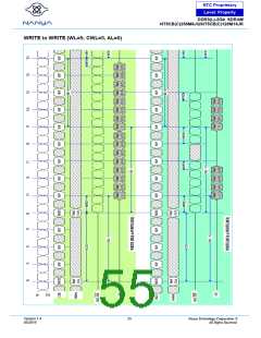
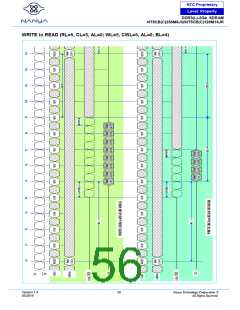
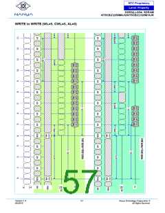
Write Operation
DDR3(L) Burst Operation
During a READ or WRITE command, DDR3(L) will support BC4 and BL8 on the fly using address A12 during the READ or
WRITE (Auto Precharge can be enabled or disabled).
A12=0, BC4 (BC4 = Burst Chop, tCCD=4)
A12=1, BL8
A12 is used only for burst length control, not as a column address.
WRITE Timing Violations
Motivation
Generally, if timing parameters are violated, a complete reset/initialization procedure has to be initiated to make sure the
DRAM works properly. However, it is desirable for certain minor violations that the DRAM is guaranteed not to “hang up”
and errors be limited to that particular operation.
For the following, it will be assumed that there are no timing violations with regard to the Write command itself (including
ODT, etc.) and that it does satisfy all timing requirements not mentioned below.
Data Setup and Hold Violations
Should the data to strobe timing requirements (tDS, tDH) be violated, for any of the strobe edges associated with a write
burst, then wrong data might be written to the memory location addressed with the offending WRITE command.
Subsequent reads from that location might result in unpredictable read data, however, the DRAM will work properly
otherwise.
Strobe to Strobe and Strobe to Clock Violations
Should the strobe timing requirements (tDQSH, tDQSL, tWPRE, tWPST) or the strobe to clock timing requirements (tDSS,
tDSH, tDQSS) be violated, for any of the strobe edges associated with a Write burst, then wrong data might be written to
the memory location addressed with the offending WRITE command. Subsequent reads from that location might result in
unpredictable read data, however the DRAM will work properly otherwise.
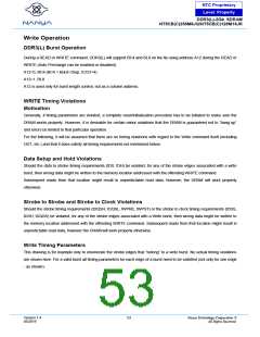
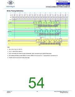
Write Timing Parameters
This drawing is for example only to enumerate the strobe edges that “belong” to a write burst. No actual timing violations
are shown here. For a valid burst all timing parameters for each edge of a burst need to be satisfied (not only for one edge
- as shown).
Version 1.4
05/2019
53
Nanya Technology Cooperation ©
All Rights Reserved.

 NANYA [ Nanya Technology Corporation. ]