analogous to voltage drops, the power dissipation out of the
LME49810 is equal to the following:
is an electrolytic type. An additional small value, high quality
film capacitor may be used in parallel with the feedback re-
sistor to improve high frequency sonic performance. If DC
offset in the output stage is acceptable without the feedback
capacitor, it may be removed but DC gain will now be equal
to AC gain.
PDMAX = (TJMAX−TAMB) / θJA
(2)
where TJMAX = 150°C, TAMB is the system ambient tempera-
ture and θJA = θJC + θCS + θSA
.
COMPENSATION CAPACITOR
The compensation capacitor (CC) is one of the most critical
external components in value, placement and type. The ca-
pacitor should be placed close to the LME49810 and a silver
mica type will give good performance. The value of the ca-
pacitor will affect slew rate and stability. The highest slew rate
is possible while also maintaining stability through out the
power and frequency range of operation results in the best
audio performance. The value shown in Figure 1 should be
considered a starting value with optimization done on the
bench and in listening testing. Please refer to Slew Rate vs.
CC Graph in Typical Performance Characteristics for de-
termining the proper slew rate for your particular application.
20216771
Once the maximum package power dissipation has been cal-
culated using Equation 2, the maximum thermal resistance,
SA, (heat sink to ambient) in °C/W for a heat sink can be
θ
calculated. This calculation is made using Equation 3 which
is derived by solving for θSA from Equation 2.
SUPPLY BYPASSING
θ
SA = [(TJMAX−TAMB)−PDMAX(θJC +θCS)] / PDMAX
(3)
The LME49810 has excellent power supply rejection and
does not require a regulated supply. However, to eliminate
possible oscillations all op amps and power op amps should
have their supply leads bypassed with low-inductance capac-
itors having short leads and located close to the package
terminals. Inadequate power supply bypassing will manifest
itself by a low frequency oscillation known as “motorboating”
or by high frequency instabilities. These instabilities can be
eliminated through multiple bypassing utilizing a large elec-
trolytic capacitor (10μF or larger) which is used to absorb low
frequency variations and a small ceramic capacitor (0.1μF) to
prevent any high frequency feedback through the power sup-
ply lines. If adequate bypassing is not provided the current in
the supply leads which is a rectified component of the load
current may be fed back into internal circuitry. This signal
causes low distortion at high frequencies requiring that the
supplies be bypassed at the package terminals with an elec-
trolytic capacitor of 470μF or more.
Again it must be noted that the value of θSA is dependent upon
the system designer's amplifier requirements. If the ambient
temperature that the audio amplifier is to be working under is
higher than 25°C, then the thermal resistance for the heat
sink, given all other things are equal, will need to be smaller.
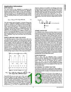
PROPER SELECTION OF EXTERNAL COMPONENTS
Proper selection of external components is required to meet
the design targets of an application. The choice of external
component values that will affect gain and low frequency re-
sponse are discussed below.
The overall gain of the amplifier is set by resistors RF and Ri
for the non-inverting configuration shown in Figure 1. The gain
is found by Equation 4 below given Ri = RIN and RF = RS.
AV = RF / Ri (V/V)
(4)
OUTPUT STAGE USING BIPOLAR TRANSISTORS
With a properly designed output stage and supply voltage of
±100V, an output power up to 500W can be generated at
0.05% THD+N into an 8Ω speaker load. With an output cur-
rent of several amperes, the output transistors need substan-
tial base current drive because power transistors usually have
quite low current gain—typical hfe of 50 or so. To increase the
current gain, audio amplifiers commonly use Darlington style
devices. Power transistors should be mounted together with
the VBE multiplier transistor on the same heat sink to avoid
thermal run away. Please see the section Biasing Tech-
nique and Avoiding Thermal Runaway for additional infor-
mation.
For best Noise performance, lower values of resistors are
used. A value of 243 is commonly used for Ri and setting the
value for RF for desired gain. For the LME49810 the gain
should be set no lower than 10V/V. Gain settings below 10V/
V may experience instability.
The combination of Ri and Ci (see Figure 1) creates a high
pass filter. The gain at low frequency and therefore the re-
sponse is determined by these components. The -3dB point
can be determined from Equation 5 shown below:
fi = 1 / (2πRiCi) (Hz)
(5)
BIASING TECHNIQUES AND AVOIDING THERMAL
RUNAWAY
If an input coupling capacitor (CIN) is used to block DC from
the inputs as shown in Figure 1, there will be another high
pass filter created with the combination of CIN and RIN. The
resulting -3dB frequency response due to the combination of
CIN and RIN can be found from equation 6 shown below:
A class AB amplifier has some amount of distortion called
Crossover distortion. To effectively minimize the crossover
distortion from the output, a VBE multiplier may be used in-
stead of two biasing diodes. The LME49810 has two dedicat-
ed pins (BIASM and BIASP) for Bias setup and provide a
constant current source of about 2.8mA. A VBE multiplier nor-
mally consists of a bipolar transistor (QMULT, see Figure 1) and
two resistors (RB1 and RB2, see Figure 1). A trim pot can also
be added in series with RB1 for optional bias adjustment. A
properly designed output stage, combine with a VBE multiplier,
fIN = 1 / (2πRINCIN) (Hz)
(6)
For best audio performance, the input capacitor should not be
used. Without the input capacitor, any DC bias from the
source will be transferred to the load. The feedback capacitor
(Ci) is used to set the gain at DC to unity. Because a large
value is required for a low frequency -3dB point, the capacitor
www.national.com
14

 NAIS [ NAIS(MATSUSHITA ELECTRIC WORKS) ]