Application Information
MUTE FUNCTION
reference voltage is not available, the following circuit using
a Zener diode can be used to power the CLPFLAG pin from
the higher supply voltage rails of the LME49810. The power
dissipation rating of RZ will need to be at-least ½W if using a
5V Zener Diode. Alternately, the following basic formula can
The mute function of the LME49810 is controlled by the
amount of current that flows into the MUTE pin. LME49810
typically requires 50μA to 100μA of mute current flowing in
order to be in “play” mode. This can be done by connecting a
reference voltage (VMUTE) to the MUTE pin through a resistor
(RM). The following formula can be used to calculate the mute
current.
be used to find the proper power rating of RZ : PDZ = (VCC
-
VZ)2/RZ (W). This formula can also be used to meet the design
requirements of any other reference voltage that the user de-
sires.
IMUTE = (VMUTE-0.7V) / (RM+10kΩ) (A)
(1)
The 10kΩ resistor value in Equation 1 is internal. Please refer
to Figure 2, LME49810 Simplified Schematic, for additional
details. For example, if a 5V voltage is connected through a
33kΩ resistor to the MUTE pin, then the mute current will be
100μA, according to Equation 1. Consequently, RM can be
changed to suit any other reference voltage requirement. The
LME49810 will enter Mute mode if IMUTE is less than 1μA
which can be accomplished by shorting the MUTE pin to
ground or by floating the MUTE pin. It is not recommended
that more than 200μA flow into the MUTE pin because dam-
age to LME49810 may occur and device may not function
properly.
20216770
THERMAL PROTECTION
The LME49810 has a thermal protection scheme to prevent
long-term thermal stress of the device. When the temperature
on the die exceeds 150°C, the LME49810 goes into thermal
shutdown. The LME49810 starts operating again when the
die temperature drops to about 145°C, but if the temperature
again begins to rise, shutdown will occur again above 150°C.
Therefore, the device is allowed to heat up to a relatively high
temperature if the fault condition is temporary, but a sustained
fault will cause the device to cycle between the thermal shut-
down temperature limits of 150°C and 145°C. This greatly
reduces the stress imposed on the IC by thermal cycling,
which in turn improves its reliability under sustained fault con-
ditions. Since the die temperature is directly dependent upon
the heat sink used, the heat sink should be chosen so that
thermal shutdown is not activated during normal operation.
Using the best heat sink possible within the cost and space
constraints of the system will improve the long-term reliability
of any power semiconductor device, as discussed in the De-
termining the Correct Heat Sink section.
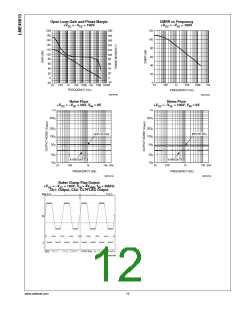
BAKER CLAMP AND CLAMP FLAG OUTPUT
The LME49810 features a Baker Clamp function with corre-
sponding CLPFLAG output pin. The clamp function keeps all
transistors in linear operation when the output goes into clip-
ping. In addition, when the output goes into clipping, a logic
low level appears at the CLPFLAG pin. The CLPFLGAG pin
can be used to drive an LED or some other visual display as
shown by Figure 1. The value of logic low voltage varies and
depends on IFLAG. For example, if IFLAG is 4.7mA then a volt-
age (VBC) of 0.4V will appear at the CLPFLAG output pin. The
smooth response of the Baker Clamp and the corresponding
CLPFLAG logic output is shown in the scope photo below:
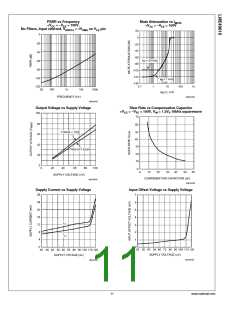
POWER DISSIPATION
When in “play” mode, the LME49810 draws a constant
amount of current, regardless of the input signal amplitude.
Consequently, the power dissipation is constant for a given
supply voltage and can be computed with the equation
PDMAX = ICC * (VCC – VEE). For a quick calculation of PDMAX
,
approximate the current to be 11mA and multiply it by the total
supply voltage (the current varies slightly from this value over
the operating range).
DETERMINING THE CORRECT HEAT SINK
The choice of a heat sink for a high-power audio amplifier is
made entirely to keep the die temperature at a level such that
the thermal protection circuitry is not activated under normal
circumstances.
20216740
+VCC = -VEE = 100V, VIN = 4VRMS, fIN = 1kHz, RC = 1kΩ
Ch1: Output, Ch2: CLPFLAG Output
The thermal resistance from the die to the outside air, θJA
(junction to ambient), is a combination of three thermal resis-
tances, θJC (junction to case), θCS (case to sink), and θSA (sink
to ambient). The thermal resistance, θJC (junction to case), of
the LME49810 is 4°C/W. Using Thermalloy Thermacote ther-
mal compound, the thermal resistance, θCS (case to sink), is
about 0.2°C/W. Since convection heat flow (power dissipa-
tion) is analogous to current flow, thermal resistance is anal-
ogous to electrical resistance, and temperature drops are
The CLPFLAG pin can source up to 10mA, and since the
CLPFLAG output is an open collector output as shown by
Figure 2, LME49810 Simplified Schematic, it should never be
left to float under normal operation. If CLPFLAG pin is not
used, then it should be connected through a resistor to a ref-
erence voltage so that IFLAG is below 10mA. For example, a
resistor of 1k can be used with a 5V reference voltage. This
will give the IFLAG of 4.7mA. In a typical LED setup, if +5V
13
www.national.com

 NAIS [ NAIS(MATSUSHITA ELECTRIC WORKS) ]