Please read CAUTION and Notice in this catalog for safety. This catalog has only typical specifications. Therefore you are requested
to approve our product specification or to transact the approval sheet for product specification, before your ordering.
P61E7.pdf 01.10.17
Chip CERAFILr SFECS Series Notice
■ Notice (Soldering and Mounting)
1. Standard Reflow Soldering Condition
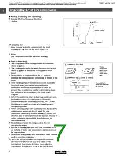
(1) Reflow
2
Peak
(240˚C max.)
240
200
Heating
(200˚C)
Pre-heating
(120-170˚C)
100
Gradual
Cooling
30 sec.
min.
30 sec.
max.
120 sec.
min.
60-120 sec.
(2) Soldering Iron
Filter shall be soldered at 280±5˚C for 3.0±0.5 seconds.
The soldering iron shall not touch the filter white soldering.
2. Wash
The component cannot be withstand washing.
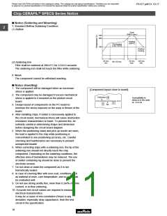
■ Notice (Handling)
1. The component will be damaged when an excessive
[Component layout close to board]
stress is applied.
2. The component may be damaged if excess mechanical
stress is applied to it mounted on the printed circuit
board.
Perforation
A
B
Susceptibility to
stress is in the order
of : A>C>B
C
Slit
3. Design layout of components on the PC board to
minimize the stress imposed on the warp or flexure of the
board.
4. After installing chips, if solder is excessively applied to
the circuit board, mechanical stress will cause destruction
resistance characteristics to lower. To prevent this, be
extremly careful in determining shape and dimension
before designing the circuit board diagram.
5. When the positioning claws and pick up nozzle are worn,
the load is applied to the chip while positioning is
concentrated to one positioning accuracy, etc. Careful
checking and maintenance are necessary to prevent
unexpected trouble.
6. When correcting chips with a soldering iron, the tip of the
soldering iron should not directly touch the chip
component. Depending on the soldering conditions, the
effective area of terminations may be reduced. The use
of solder containing Ag should be done to prevent the
electrode erosion.
7. Do not clean or wash the component as it is not
hermetically sealed.
8. In case of covering filter with over coat, conditions such
as material of resin, cure temperature, and so on should
be evaluated well.
9. Do not use strong acidity flux, more than 0.2wt% chlorine
content, in re-flow soldering.
10. Accurate test circuit values are required to measure
electrical characteristics.
It may be a cause of mis-correlation if there is any
deviation, especially stray capacitance, from the test
circuit in the specification.
10

 MURATA [ muRata ]