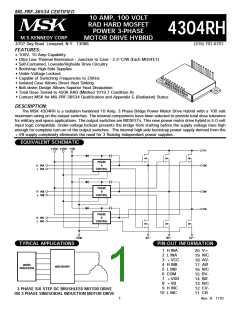
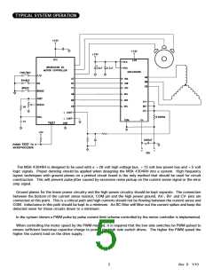
APPLICATION NOTES
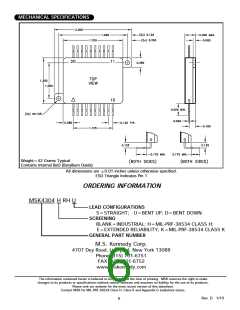
MSK 4304RH PIN DESCRIPTIONS
UVLO - The under voltage lockout function of the MSK
4304RH prevents the device from starting before sufficient
bias voltage is available. The UVLO feature monitors the
VDD supply and holds the outputs low until the voltage
level rises above the threshold during start up. After start
up the UVLO circuit will hold the low side switches off if
VDD falls below the threshold but the high side switches
will not be controlled by UVLO after start up.
+ VCC - Is the low voltage supply for the lowside driv-
ers. A 0.1 µF ceramic capacitor in parallel with a 10µF
tantalum capacitor is the recommended bypassing from
the + VCC pin to the COM pin.
+ VDD - Is the low voltage supply for the input logic to
the hybrid. A 0.1 µF ceramic capacitor in parallel with
a 4.7µF tantalum capacitor is the recommended by-
passing to the COM pin.
MAXIMUM DUTY CYCLE AND HIGH SIDE BIAS - The MSK
4304RH uses three independent bootstrap circuits to power
each of the high side switches. When the switches are
turned on the high side drivers are powered by the charge
in the bootstrap capacitors. The voltage on the bootstrap
capacitors has an initial 1.2V drop and decays at a rate of
approximately 0.5V every 100µS. The voltage can be ap-
proximated by the equation:
+ VB - Is the connection used to provide power to the
floating high-side bootstrap supplies in the gate drive
circuitry.
V+ - Is the high voltage positive rail connection to the
tops of the three half bridges. Proper power supply
bypassing must be connected from this pin to the COM
pin for good filtering. This bypassing must be done as
close to the hybrid as possible. + VCC, + VDD and + VB
should be present and stable whenever V+ is present.
VBS = + VB - 1.2V - 5 x TON
TON is the switch on time in mS
VBS is the bootstrap capacitor voltage
VBS should be greater than or equal to 10 volts for maxi-
mum gate drive. If VBS falls too low loss of high side con-
trol my result.
H INA, H INB, H INC - Are active high logic inputs for
signalling the corresponding phase high-side switch to
turn on. The logic inputs are compatible with standard
LSTTL/CMOS outputs. These inputs are clamped to VDD
and COM, they must be limited to less than 10mA if
they are allowed to exceed those limits.
The lowside switches must be activate every cycle or held
active during static operation to provide a return path for
charging the highside bootstrap capacitor and prevent loss
of highside control.
L INA, L INB, L INC - Are active high inputs for signal-
ling the corresponding phase low-side switch to turn
on. The logic inputs are compatible w ith standard
LSTTL/CMOS outputs. These inputs are clamped to VDD
and COM, they must be limited to less than 10mA if
they are allowed to exceed those limits.
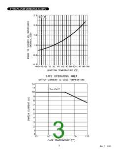
TOTAL DOSE RADIATION TEST
PERFORMANCE
Radiation performance curves for TID testing have been
generated for all radiation testing performed by MS Kennedy.
These curves show performance trends throughout the TID
test process and can be located in the MSK 4304RH radia-
tion test report. The complete radiation test report is avail-
able in the RAD HARD PRODUCTS section on the MSK
w ebsite.
AØ, BØ, CØ - Are the pins connecting the 3 phase
bridge switch outputs.
AV-, BV-, CV- - Are the connections from the bottoms
of the three half bridges. These pins get connected to
the COM pin. If current sensing is desired they may be
connected to the COM pin through a low value sense
resistor.
http://www.mskennedy.com/store.asp?pid=9951&catid=19680
COM - Is the connection that all hybrid power supply
connections are returned to and bypassed to.
Rev. D 1/10
4

 MSK [ M.S. KENNEDY CORPORATION ]