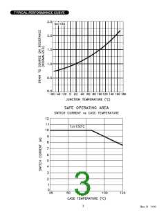
7
ABSOLUTE MAXIMUM RATINGS
9
High Voltage Supply
Logic Supply
Logic Input Voltage
Logic Input Current
Lowside Supply
-65° to + 150° C
300° C
V+
100V
18V
VDD
10mA
18V
18V
Storage Temperature Range
Lead Temperature Range
(10 Seconds)
Case Operating Temperature
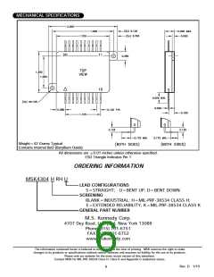
MSK 4304RH
TsT
TLD
TC
+ VDD
VH/LIN
IH/LIN
+ VCC
+ VB
IOUT
-40° C to + 85° C
-55° C to + 125° C
+ 150° C
Highside Supply
MSK 4304K/H/E RH
J unction Temperature
Continuous Output Current
Peak Output Current
Thermal Resistance @ 125° C
10A
14A
TJ
IPK
θJ C
(Output Switches,J unction to Case)
2.5° C/W
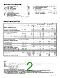
ELECTRICAL SPECIFICATIONS
3
2
GROUP A
SUBGROUP
5
MSK 4304K/H/E RH
Min. Typ. Max.
MSK 4304RH
UNITS
Parameters
8
Test Conditions
Min. Typ. Max.
OUTPUT CHARACTERISTICS
-
-
-
-
-
-
-
-
-
-
0.08
-
-
1.6
-
-
25
-
1
2
3
1
-
-
-
-
-
-
-
-
-
-
-
-
-
0.08
0.16
0.08
1.5
2.4
1.2
25
250
25
-
-
-
Ω
Ω
Ω
volts
volts
volts
µA
µA
µA
nS
Drain-Source ON Resistance 1
IDS= 10A
IDS= 10A
(each MOSFET) (for thermal calculations only)
0.8
1.4
0.6
1
10
1
0.8
-
-
1
-
-
Drain-Source Voltage (VDS(on))
(each MOSFET)
1
2
1
3
V+ = 80V
V+ = 80V
V+ = 80V
1
2
3
-
Leakage Current (Each MOSFET)
-
Reverse Recovery Time 1
ID= 10A, di/dt= 100A/µS
-
370
-
370
BIAS SUPPLY CHARACTERISTICS
-
-
-
-
-
-
-
-
-
-
0.02
-
0.02
-
2
6
2
6
9
0.02
-
0.02
-
2
6
2
6
9
mA
mA
mA
mA
mA
1,3
2
1,3
2
+ VCC= 15V
+ VCC Bias Current
+ VB Bias Current
+ VB= 15V
+ VDD Bias Current
+ VDD= 15V
4.5
4.5
1,2,3
INPUT SIGNAL CHARACTERISTICS
-
0.8
8.0
-
-10
-
Positive Trigger Threshold Voltage
Negative Trigger Threshold Voltage
+ VCC= 15V
+ VCC= 15V
+ VDD
-
0.8
8.0
-
-10 -1.2
-
-
2.3
1.8
10
3.0
-
12.0
75
-
2.3 3.0
1.8
10 12.0
1
1
-
-
volts
volts
volts
µA
µA
µJ
-
6
Under-voltage Lockout
1,2,3
1,2,3
1,2,3
4
VIN= + 5V
25
25
75
-
All Inputs
Logic Input Current
VIN= 0V
E(ON)
E(OFF)
-1.2
TBD
TBD
TBD
TBD
-
-
-
-
1
Switching Loss Inductive Load
-
4
µJ
NOTES:
Guaranteed by design but not tested. Typical parameters are representative of actual device performance but are for reference only.
Industrial grade and "E" suffix devices shall be tested to subgroups 1 unless otherwise specified.
Space and Military grade devices ("K & H" suffix) shall be 100% tested to subgroups 1, 2 and 3.
Subgroups 5 and 6 testing available upon request.
1
2
3
4
5
Subgroup 1, 4 TA= TC= + 25° C
2, 5 TA= TC= + 125° C
3, 6 TA= TC= -55° C
See UVLO paragraph in the application notes section.
6
7
8
9
Continuous operation at or above absolute maximum ratings may adversely effect the device performance and/or life cycle.
Pre and post irradiation limits at 25° C, up to 300Krad TID, are identical unless otherwise specified.
When applying power to the device, apply the low voltage followed by the high voltage or alternatively,apply both at the same time.
Do not apply high voltage without low voltage present.
2
Rev. D 1/10

 MSK [ M.S. KENNEDY CORPORATION ]