8
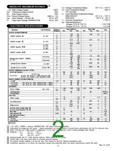
ABSOLUTE MAXIMUM RATINGS
Storage Temperature Range
Lead Temperature Range
(10 Seconds)
Case Operating Temperature Range
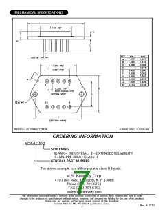
MSK4 2 0 6 H/E
MSK4 2 0 6
J unction Temperature
Thermal Resistance
-65° C to + 150° C
3 0 0 ° C
TST
TLD
High Voltage Supply
Continuous Output Current
Peak Output Current
Output Voltage Range
Input Voltage, + IN and -IN
Logic Input Voltage (SHDN/FILTER)
1 0 0 V
2 0 A
3 0 A
+ VS
IOUT
IPK
VOUT
VIN
TC
-55° C to + 125° C
-40° C to + 85° C
+ 1 5 0 ° C
GND to + Vs
0V to 12V
0V to 10V
TJ
θJc
VL
(Output FETS @ 125° C)
(Output FETS @ 25° C)
1.25° C/W
1.0° C/W
ELECTRICAL SPECIFICATIONS
NOTES:
1
2
3
4
+ Vs= 28V, I SENSE= Ground, SHDN/FILTER= 0V unless otherw ise specified.
Guaranteed by design but not tested. Typical parameters are representative of actual device performance but are for reference only.
Class H devices are 100% tested to subgroups 1,2,3,4, and 7. Subgroup 5 and 6 testing available upon request.
Subgroup 1,4,7
TA= TC= + 25° C
TA= TC= + 125° C
TA= TC= -55° C
2,5
3,6
5
6
7
8
Industrial grade and "E" suffix devices shall be 100% tested at 25° C only.
Tested with a low duty cycle pulse to minimize junction heating.
The typical internal reading is for the die only. This should be used for thermal calculations only.
Continuous operation at or above the maximum ratings may adversely effect the device performance and/or life cycle.
Rev. B 2/10
2

 MSK [ M.S. KENNEDY CORPORATION ]