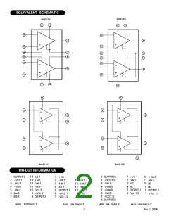
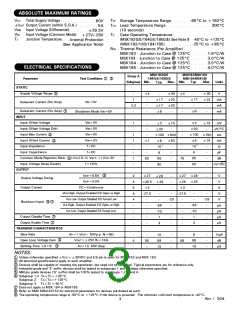
APPLICATION NOTES
THERMAL PROTECTION:
The amplifiers are equipped with thermal protection circuitry
that protects each amplifier from damage caused by excessive
junction temperature. The output is disabled when the junction
temperature reaches approximately 160°C. After the junction
temperature cools to approximately 140°C, the output is again
enabled. The thermal protection may cycle on and off depend-
ing on the output load and signal conditions; this may have an
undesirable effect on the load.
POWER SUPPLIES:
For the MSK 182/183/184/185 maximum total supply volt-
age is specified as 60V. However, dual and unbalanced power
supply operation is permissible as long as total supply voltage
does not exceed 60V.
POWER SUPPLY BYPASSING:
It should be noted that even though this internal protection
circuitry does protect against overload conditions, it does not
take the place of proper heat sinking. For reliable operation,
junction temperature should be limited to 150°C, maximum.
Power supply terminals must be effectively decoupled with a
high and low frequency bypass circuit to avoid power supply
induced oscillation. An effective decoupling scheme consists
of a 0.1µF ceramic capacitor in parallel with a 10µF tantalum
capacitor for each power supply pin to ground. In addition, it is
recommended that a 0.01µF capacitor be placed between Vcc
as close to the amplifiers as possible.
ENABLE/STATUS PIN:
For the MSK 182 and MSK 183 this pin actually has a dual
function. First, when the pin is forced low, the output stage is
disabled. Second, it can be monitored to determine if the device
is in thermal shutdown. These functions can be used on the
same device with either single or dual supplies. For normal
operation, the E/S pin must be left open or pulled at least 2.4
volts above the negative rail. In noisy applications, a small value
capacitor between the E/S pin and -Vcc may be required.
To disable the output, the user must pull the E/S pin low, no
greater than 0.8V above -Vcc. To once again enable the device,
the E/S pin must be brought at least 2.4 volts above -Vcc or be
disconnected. It should be noted that when the E/S pin is high,
the internal thermal shutdown is still active.
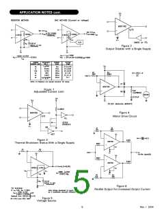
CURRENT LIMIT:
The MSK 182 and MSK 183 offer accurate, user-selectable
current limit. Unlike typical designs that use a power resistor in
series with the output to sense load, the MSK 182 and MSK
183 sense the load indirectly and therefore do not require a
resistor to handle the full output current. Current limit is se-
lected by controlling the input to the ILIM pin.
The easiest method is to use a resistor or potentiometer
connected between -Vcc and the ILIM pin. Use the following
equation to select proper resistor value:
71,250
-13.75KΩ
Rcc=
If the E/S pin is used to monitor thermal shutdown, during
normal operation the voltage on the E/S pin is typically 3.5V
above -Vcc. Once shutdown has occurred this voltage will drop
to approximately 350mV above -Vcc. This function is not avail-
able on the MSK 184 or the MSK 185.
ILIM
A low level control signal (0-330µA) can also be used to con-
trol the current level digitally. If the pin is left open, the current
is programmed to OA, while connecting ILIM directly to -Vcc
sets the output current to it's maximum, typically 5A. Such is
the case with the MSK 184 or the MSK 185.
COMPENSATION:
SAFE OPERATING AREA:
For normal operation output compensation is not typically
required. However, if the MSK 182 or MSK 183 is intended to
be driven into current limit the user may find that an R/C net-
work is required. A snubber network from the output to ground
for each amplifier will provide stability. If driving large capaci-
tive or inductive loads, a snubber network will also enhance
stability. Typically 3Ω to 10Ω in series with 0.01µF is accept-
able.
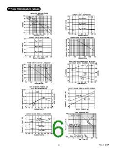
The safe operating area curve is a graphical representation of
the power handling capability of the amplifier under various
conditions. Power dissipation of the device is equal to the prod-
uct of the voltage across the output transistor times the output
current. As can be seen in the curve on page 6, safe operating
current decreases with an increase in temperature as well as an
increase in the voltage across the output transistor. Therefore,
for maximum amplifier performance it is important to keep case
temperature as low as possible and to keep Vcc as close to
the output rail as achievable.
APEX PA26 REPLACEMENT:
The MSK 185 is a hermetically sealed, hi-reliability, pin simi-
lar replacement for the APEX PA26. The supply voltage input
and output pin configurations are identical. However, the VBOOST
and ISENSE functions are not available with the MSK 185. The
VBOOST and ISENSE pins of the PA26 have no internal connec-
tion on the MSK 185. Therefore, any external circuitry con-
nected to pins 3,4,9 & 10 will not degrade the performance of
the MSK 185.
The MSK 185 also provides 4-40 isolated mounting studs in
place of the mounting holes of the PA26. These mounting
studs, which are brazed to the package bottom, offer excellent
heat sink mounting performance while decreasing the potential
amplifier/package damage sometimes experienced with mount-
ing holes.
TYPICAL CONNECTION DIAGRAM
Rev. I 3/04
4

 MSK [ M.S. KENNEDY CORPORATION ]