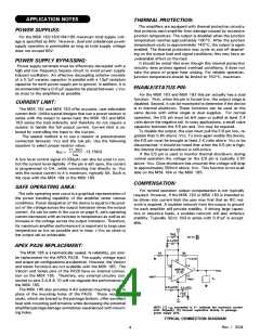
ABSOLUTE MAXIMUM RATINGS
VCC
IOUT
Total Supply Voltage
TST
TLD
Storage Temperature Range
Lead Temperature Range
(10 seconds)
-65°C to +150°C
300°C
60V
5A
29.5V
+27V/-29V
Output Current (within S.O.A.)
Input Voltage (Differential)
Input Voltage (Common Mode)
Junction Temperature
VIND
VIN
TJ
TC
Case Operating Temperature
(MSK182G/E/184G/E/185G/E) See Note 9 -40°C to +125°C
Internal Protection
(MSK182/183/184/185)
-25°C to +85°C
(See Application Note)
RTH
Thermal Resistance (Per Amplifier)
MSK182 - Junction to Case @ 125°C
MSK183 - Junction to Case @ 125°C
MSK184 - Junction to Case @ 125°C
MSK185 - Junction to Case @ 125°C
1.8°C/W
3.0°C/W
3.5°C/W
4.0°C/W
ELECTRICAL SPECIFICATIONS
MSK182G/E
184G/E/185G/E
MSK182/MSK183/
MSK184/MSK185
Group A
Test Conditions
Parameter
1
2
Subgroup
Max. Min.
Typ.
Max.
Units
Min.
Typ.
STATIC
Supply Voltage Range
-
± 17
-
± 3±
V
3
-
1
± 4
± 3±
± 2±
± 2±
-
± 4
-
-
-
-
± 23
mA
mA
mA
-
-
-
± 17
± 17
± 6
Quiescent Current (Per Amp)
VIN=±V
2,3
-
-
-
Quiescent Current (Per Amp)
7
± 6
Shutdown Mode VIN=±V
INPUT
Input Offset Voltage
VIN=±V
1
-
± 1±
-
-
± 2
± 15
-
mV
µV/°C
nA
-
± 2
± 3±
± 1±±
± 5
1± 7
6
Input Offset Voltage Drift
VIN=±V
± 3±
-
-
Input Bias Current
VIN=±V
3
1
1
-
± 5±±
-
± 1±± ± 75±
-
± 1
-
Input Offset Current
Input Impedance
VIN=OV
-
± 5
1±7
6
± 75
nA
± 5±
3
f=DC
f=DC
-
-
-
-
-
-
-
-
-
Ω
Input Capacitance
-
-
pF
-
Common Mode Rejection Ratio
Input Voltage Noise Density
(-VCC)-±01≤ VIN ≤ (+VCC)-3V
f=1KHZ
95
9±
dB
3
1
-
8±
-
75
-
95
nV/√HZ
9±
OUTPUT
3
IOUT=±06A
IOUT=30±A
4
4
4
4
4
-
-
± 27 ± 28
± 25 ± 26
-
V
V
± 27
± 28
Output Voltage Swing
Output Current
-
± 2505 ± 26
-
DC=Continuous
± 3
-
-
-
A
± 3
-
-
-
V
E/S High- Output Enabled E/S Open or High
-2705
-
V
-2705
-
VE/S Low- Output Disabled E/S Forced Low
-
-
-
-
-
-
-29
V
-
-
-
-
-
-
-29
Shutdown Input 3
7
I
E/S High- Output Enabled E/S Open or High
-65
-7±
1
-
-
-
-
µA
µA
µS
µS
-
-
-
-
-65
-7±
1
IE/S Low- Output Disabled E/S Forced Low
-
Output Disable Time
Output Enable Time
7
-
7
3
-
3
TRANSFER CHARACTERISTICS
Slew Rate
AV=1 VOUT= 5±Vp-p RL=8Ω
VOUT=± 25V RL=1KΩ
AV=1± 5±V Step
-
4
-
-
-
-
-
88
-
8
-
-
-
V/µS
dB
-
9±
-
1±
98
15
3
Open Loop Voltage Gain
Settling Time ± ±01ꢀ
98
18
3
µS
NOTES:
1 Unless otherwise specified ± VCC= ± 3±VDC and E/S pin is open for MSK 182 and MSK 1830
2 All electrical specifications apply to each amplifier0
3 Devices shall be capable of meeting the parameter, but need not to be tested0 Typical parameters are for reference only0
4 Industrial grade and 'E' suffix devices shall be tested to subgroups 1 and 4 unless otherwise specified0
5 Military grade devices ('G' suffix) shall be 1±±ꢀ tested to subgroups 1,2,3 and 40
6 Subgroup 1,4 TA=TC=+25°C
Subgroup 2 TA=TC=+125°C
Subgroup 3 TA=TC=-4±°C
7 Does not apply to MSK 184 or MSK1850
8 Refer to SMD 5962-92152 for electrical parameters for devices purchased as such0
9 The operating temperature range is -55°C to +125°C if the device is powered0 The minimum cold start temperature is -4±°C0
Rev. I 3/04
3

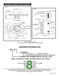
 MSK [ M.S. KENNEDY CORPORATION ]