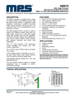
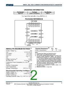
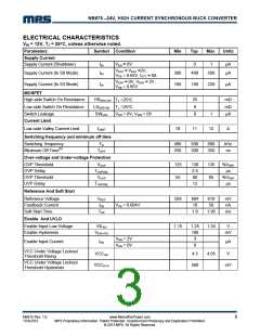
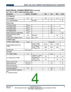
NB675 –24V, HIGH CURRENT SYNCHRONOUS BUCK CONVERTER
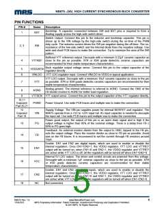
PIN FUNCTIONS
PIN #
Name
Description
Bootstrap. A capacitor connected between SW and BST pins is required to form a
floating supply across the high-side switch driver.
1
BST
Switch Output. Connect this pin to the inductor and bootstrap capacitor. This pin is
driven up to the VIN voltage by the high-side switch during the on-time of the PWM
duty cycle. The inductor current drives the SW pin negative during the off-time. The on-
resistance of the low-side switch and the internal diode fixes the negative voltage. Use
wide and short PCB traces to make the connection. Try to minimize the area of the SW
pattern.
2, 3
SW
Buffered VTT reference output. Decouple with a minimum 0.22μF ceramic capacitor as
4
VTTREF close to the pin as possible. X7R or X5R grade dielectric ceramic capacitors are
recommended for their stable temperature characteristics.
Buck regulator output voltage sense. Connect this pin to the output capacitor of the
regulator directly
5
6
VDDQSEN
VINLDO
VTT
VTT LDO regulator input. Connect VINLDO to VDDQ in typical application.
VTT LDO output. Decouple with a minimum 10uF ceramic capacitor as close to the pin
as possible. X7R or X5R grade dielectric ceramic capacitors are recommended for their
stable temperature characteristics.
7
Analog ground. The internal reference is referred to AGND. Connect the GND of the
FB divider resistor to AGND for better load regulation.
8
9
AGND
VTTSEN VTT output sense. Connect this pin to the output capacitor of the VTT regulator directly
10,11
Exposed
Pad 20,21
PGND
VIN
Power Ground. Use wide PCB traces and multiple vias to make the connection.
12
Exposed
Pad 19
Supply Voltage. The VIN pin supplies power for internal MOSFET and regulator. The
NB675 operate from a +5V to +22V input rail. An input capacitor is needed to decouple
the input rail. Use wide PCB traces and multiple vias to make the connection.
Power good output, the output of this pin is an open drain signal and is high if the
output voltage is higher than 95% of the nominal voltage. There is a delay from FB ≥
95% to PG goes high.
13
PG
Feedback. An external resistor divider from the output to GND, tapped to the FB pin,
sets the output voltage. Place the resistor divider as close to FB pin as possible. Avoid
vias on the FB traces. It is recommend to set the current through FB resistors around
10uA.
14
FB
Enable. EN1 and EN2 are digital inputs, which are used to enable or disable the
internal regulators. Once EN1=EN2=1, the VDDQ regulator, VTT LDO and VTTREF
output will be turned on; when EN1=0 and EN2=1, the VDDQ regulator and VTTREF
are active while VTT LDO is off; all the regulators will be turned off when EN1=EN2=0.
15
16
EN1
VCC
Internal 5V LDO output. The driver and control circuits are powered from this voltage.
Decouple with a minimum 1µF ceramic capacitor as close to the pin as possible. X7R
or X5R grade dielectric ceramic capacitors are recommended for their stable
temperature characteristics.
Enable. EN1 and EN2 are digital inputs, which are used to enable or disable the
internal regulators. Once EN1=EN2=1, the VDDQ regulator, VTT LDO and VTTREF
output will be turned on; when EN1=0 and EN2=1, the VDDQ regulator and VTTREF
are active while VTT LDO is off; all the regulators will be turned off when EN1=EN2=0.
17
18
EN2
NC
Not connected.
NB675 Rev. 1.0
1/14/2013
www.MonolithicPower.com
MPS Proprietary Information. Patent Protected. Unauthorized Photocopy and Duplication Prohibited.
© 2013 MPS. All Rights Reserved.
5

 MPS [ MONOLITHIC POWER SYSTEMS ]