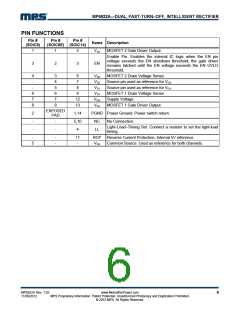
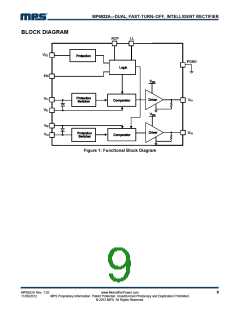
MP6922A—DUAL, FAST-TURN–OFF, INTELLIGENT RECTIFIER
OPERATION
The MP6922A operates in discontinuous-
conduction mode (DCM), continuous-conduction
mode (CCM), and critical conduction mode
(CrCM) condition. Operating in either DCM or
CrCM, the control circuitry controls the gate in
forward mode; it turns the gate off when the
MOSFET current is low. In CCM, the control
circuitry turns off the gate during very fast
transients.
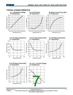
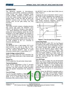
the MOSFET turns on after about 200ns turn-on
delay (Figure 2).
Triggering the turn-on threshold (-30mV) causes
the circuit to add a blanking time (minimum on-
time 1μs), during which the turn-off threshold
changes from +30V to +100mV. This blanking
time avoids erroneous triggering caused by
ringing on the synchronous power switch.
Blanking
0mV
The control circuitry contains a blanking function
that ensure that when the MOSFET turns
ON/OFF, the MOSFET remains in that state for
~1μs, which determines the minimum ON-time.
During the turn-on blanking period, the turn-off
threshold is not totally blanked, but changes to
~+100mV (instead of +30mV). This ensures that
the part can always turn OFF even during the
turn-on blanking period (albeit slower, so avoid
setting the synchronous period to less than 1μs
at CCM condition in the LLC converter to
eliminate shoot-through).
-30mV
VDS
tDon
tDoff
VGATE
2V
Figure 2: Turn-On and Turn-Off delay
Conducting Phase
When the MOSFET turns ON, VDS (-ISD×RDS(ON)
)
VD Clamp
rise relative to the switch current (ISD) drop. When
VDS rises above the turn-on threshold (–30mV),
the control circuitry stops pulling up the gate
driver and the MOSFET driver voltage drops,
which increases the MOSFET’s RDS(ON). This
adjusts VDS (-ISD×RDS(ON)) to around -30mV even
when the switch current ISD is fairly small, and
can prevent the internal driver from triggering
until the current through the MOSFET has
dropped to near zero.
The MP6922A uses a high-voltage JFET at its
input because VD1,2 can go as high as 180V.
Connect a small resistor between the VD1,2 pin
and the external MOSFET drain to avoid
excessive currents when VG goes below -0.7V.
Under-Voltage Lockout (UVLO)
When VDD goes below the UVLO threshold, the
part enters sleep mode and a 10kꢀ resistor pulls
down VG.
Turn-Off Phase
Enable Pin
When VDS rises to trigger the turn-off threshold
(30mV), the control circuitry pulls down the driver
switch voltage after a 20ns turn-off delay (shown
in Figure 2). Similarly, a 1.6μs blanking time
occurs after the switch turns off, during which the
MOSFET does not turn on to avoid erroneous
triggering.
If EN is pulled low, the part enters sleep mode.
Thermal Shutdown
If the junction temperature of the IC exceeds
150°C, VG is pulled low and the part stops
switching. The part resumes normal operation
after the junction temperature has dropped to
120°C.
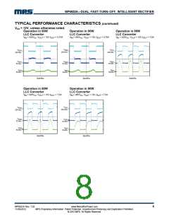
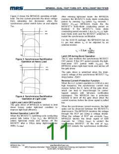
Figure 3 shows the MP6922A operating under a
heavy-load. The high current initially saturates
the driver voltage. After VDS goes above –30mV,
the driver voltage decreases to adjust the VDS to
around –30mV.
Turn-On Phase
VDS (VD–VSS) goes negative (<-500mV) when the
switch current flows through the MOSFET’s body
diode. If VDS is much lower than the turn-on
threshold of the control circuitry (-30mV), then
MP6922A Rev. 1.02
11/30/2012
www.MonolithicPower.com
MPS Proprietary Information. Patent Protected. Unauthorized Photocopy and Duplication Prohibited.
© 2012 MPS. All Rights Reserved.
10

 MPS [ MONOLITHIC POWER SYSTEMS ]