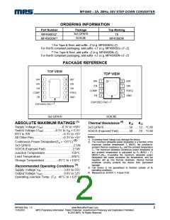
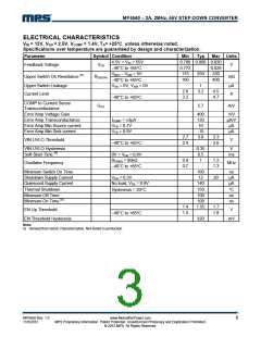
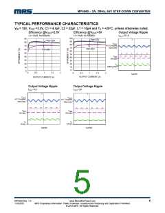
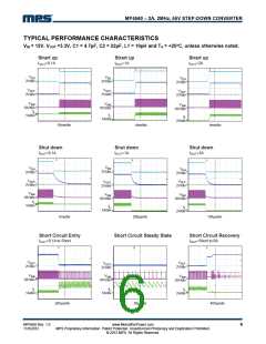
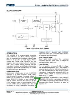
MP4560 – 2A, 2MHz, 55V STEP-DOWN CONVERTER
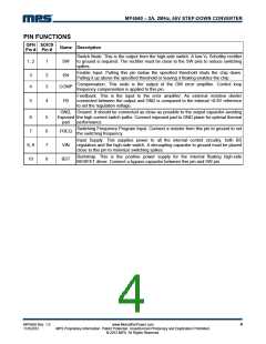
PIN FUNCTIONS
QFN SOIC8
Pin # Pin #
Name Description
Switch Node. This is the output from the high-side switch. A low VF Schottky rectifier
to ground is required. The rectifier must be close to the SW pins to reduce switching
spikes.
1, 2
1
SW
Enable Input. Pulling this pin below the specified threshold shuts the chip down.
Pulling it up above the specified threshold or leaving it floating enables the chip.
3
4
2
3
EN
Compensation. This node is the output of the GM error amplifier. Control loop
frequency compensation is applied to this pin.
COMP
Feedback. This is the input to the error amplifier. An external resistive divider
connected between the output and GND is compared to the internal +0.8V reference
to set the regulation voltage.
5
4
FB
GND, Ground. It should be connected as close as possible to the output capacitor avoiding
Exposed the high current switch paths. Connect exposed pad to GND plane for optimal thermal
6
7
5
6
7
8
pad
performance.
Switching Frequency Program Input. Connect a resistor from this pin to ground to set
the switching frequency.
FREQ
Input Supply. This supplies power to all the internal control circuitry, both BS
regulators and the high-side switch. A decoupling capacitor to ground must be placed
close to this pin to minimize switching spikes.
8, 9
10
VIN
Bootstrap. This is the positive power supply for the internal floating high-side
MOSFET driver. Connect a bypass capacitor between this pin and SW pin.
BST
MP4560 Rev. 1.0
11/5/2012
www.MonolithicPower.com
MPS Proprietary Information. Patent Protected. Unauthorized Photocopy and Duplication Prohibited.
© 2012 MPS. All Rights Reserved.
4

 MPS [ MONOLITHIC POWER SYSTEMS ]