MP4560 – 2A, 2MHz, 55V STEP-DOWN CONVERTER
ORDERING INFORMATION
Part Number
MP4560DQ*
MP4560DN**
Package
3x3 QFN10
SOIC8E
Top Marking
T8
MP4560DN
* For Tape & Reel, add suffix –Z (e.g. MP4560DQ–Z).
For RoHS compliant packaging, add suffix –LF (e.g. MP4560DQ–LF–Z)
** For Tape & Reel, add suffix –Z (e.g. MP4560DN–Z).
For RoHS compliant packaging, add suffix –LF (e.g. MP4560DN–LF–Z)
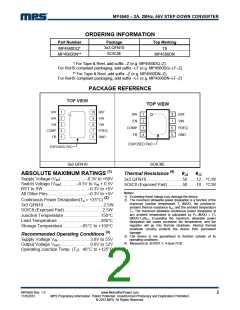
PACKAGE REFERENCE
TOP VIEW
TOP VIEW
SW
SW
1
2
3
4
5
10 BST
SW
EN
1
2
3
4
8
7
6
5
BST
9
8
7
6
VIN
VIN
EN
VIN
COMP
FB
FREQ
GND
COMP
FB
FREQ
GND
EXPOSED PAD
EXPOSED PAD
3x3 QFN10
SOIC8E
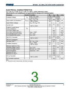
ABSOLUTE MAXIMUM RATINGS (1)
Supply Voltage (VIN).....................–0.3V to +60V
Switch Voltage (VSW)............ –0.5V to VIN + 0.5V
BST to SW.....................................–0.3V to +5V
All Other Pins.................................–0.3V to +5V
Thermal Resistance (4)
3x3 QFN10..............................50 ...... 12...°C/W
SOIC8 (Exposed Pad) ............50 ...... 10...°C/W
θJA
θJC
Notes:
1) Exceeding these ratings may damage the device.
2) The maximum allowable power dissipation is a function of the
maximum junction temperature TJ (MAX), the junction-to-
ambient thermal resistance θJA, and the ambient temperature
TA. The maximum allowable continuous power dissipation at
any ambient temperature is calculated by PD (MAX) = (TJ
(MAX)-TA)/θJA. Exceeding the maximum allowable power
dissipation will cause excessive die temperature, and the
regulator will go into thermal shutdown. Internal thermal
shutdown circuitry protects the device from permanent
damage.
(2)
Continuous Power Dissipation(TA = +25°C)
3x3 QFN10……………………………………2.5W
SOIC8 (Exposed Pad)………………………2.5W
Junction Temperature...............................150°C
Lead Temperature ....................................260°C
Storage Temperature.............. –65°C to +150°C
Recommended Operating Conditions (3)
Supply Voltage VIN ...........................3.8V to 55V
Output Voltage VOUT.........................0.8V to 52V
Operating Junction Temp. (TJ). -40°C to +125°C
3) The device is not guaranteed to function outside of its
operating conditions.
4) Measured on JESD51-7, 4-layer PCB.
MP4560 Rev. 1.0
11/5/2012
www.MonolithicPower.com
MPS Proprietary Information. Patent Protected. Unauthorized Photocopy and Duplication Prohibited.
© 2012 MPS. All Rights Reserved.
2

 MPS [ MONOLITHIC POWER SYSTEMS ]