MP4558 – 1A, 2MHz, 55V STEP-DOWN CONVERTER
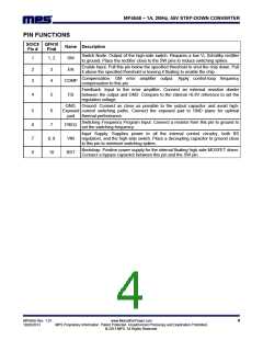
PIN FUNCTIONS
SOIC8 QFN10
Name Description
Pin #
Pin#
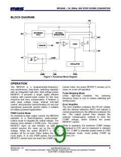
Switch Node. Output of the high-side switch. Requires a low VF Schottky rectifier
to ground. Place the rectifier close to the SW pins to reduce switching spikes.
1
1, 2
SW
EN
Enable Input. Pull this pin below the specified threshold to shut the chip down. Pull
it above the specified threshold or leaving it floating to enable the chip.
2
3
3
4
Compensation. GM error amplifier output. Apply control-loop frequency
compensation to this pin.
COMP
Feedback. Input to the error amplifier. Connect an external resistive divider
between the output and GND: Compare to the internal +0.8V reference to set the
regulation voltage.
4
5
FB
GND, Ground. Connect as close as possible to the output capacitor and avoid high-
Exposed current switching paths. Connect the exposed pad to GND plane for optimal
5
6
7
8
6
7
pad
thermal performance.
Switching Frequency Program Input. Connect a resistor from this pin to ground to
set the switching frequency.
FREQ
Input Supply. Supplies power to all the internal control circuitry, both BS
regulators, and the high-side switch. Place a decoupling capacitor to ground close
to this pin to minimize switching spikes.
8, 9
10
VIN
Bootstrap. Positive power supply for the internal floating high-side MOSFET driver.
Connect a bypass capacitor between this pin and the SW pin.
BST
MP4558 Rev. 1.01
10/28/2013
www.MonolithicPower.com
MPS Proprietary Information. Patent Protected. Unauthorized Photocopy and Duplication Prohibited.
© 2013 MPS. All Rights Reserved.
4

 MPS [ MONOLITHIC POWER SYSTEMS ]