MP2144 – 2A, 5.5V, 1.2MHz. 40μA IQ, SYNCHRONOUS STEP-DOWN SWITCHER
VOUT
VOUT
⎛
⎞
The input voltage ripple caused by capacitance
can be estimated by:
ΔVOUT
=
× 1−
×RESR
⎜
⎟
⎠
fS ×L1
V
IN
⎝
⎛
⎞
⎟
⎠
ILOAD
VOUT
VOUT
The characteristics of the output capacitor also
affect the stability of the regulation system.
ΔV =
×
× 1−
⎜
IN
fS ×C1
V
IN
V
⎝
IN
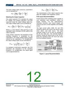
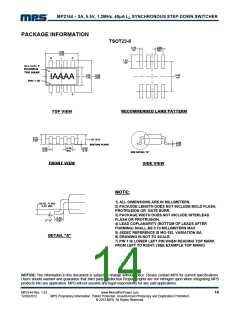
PCB Layout Recommendation
Selecting the Output Capacitor
Proper layout of the switching power supplies is
very important, and sometimes critical for
proper function. For the high-frequency
switching converter, poor layout design can
result in poor line or load regulation and stability
issues.
The output capacitor (C2) maintains the output
DC voltage. Use Ceramic capacitors. Low ESR
capacitors keep the output voltage ripple low.
The output voltage ripple can be estimated by:
⎛
⎞ ⎛
VOUT
⎞
⎟
⎠
VOUT
1
ΔVOUT
=
× 1−
× R
⎟ ⎜
+
⎜
ESR
fS ×L1
V
8× fS ×C2
⎝
IN ⎠ ⎝
The high current paths (GND, IN, and SW)
should be placed very close to the device using
short, direct, and wide traces. The input
capacitor needs to be as close as possible to
the IN and GND pins. The external feedback
resistors should be placed next to the FB pin.
Keep the switching node SW short and away
from the feedback network.
Where L1 is the inductor value and RESR is the
equivalent series resistance (ESR) value of the
output capacitor.
Using ceramic capacitors, the impedance at the
switching frequency is dominated by the
capacitance. The output voltage ripple is mainly
caused by the capacitance. For simplification,
the output voltage ripple can be estimated by:
OUT
R4
SW
L1
⎛
⎞
⎟
⎠
VOUT
VOUT
ΔVOUT
=
× 1−
R3
⎜
2
VIN
V
8× fS ×L1 ×C2
⎝
IN
1
8
2
3
4
7
6
For tantalum or electrolytic capacitors, the ESR
dominates the impedance at the switching
frequency. For simplification, the output ripple
can be approximated as:
5
GND
C1A C1
Figure 3: Layout Recommendation
MP2144 Rev. 1.03
12/20/2012
www.MonolithicPower.com
MPS Proprietary Information. Patent Protected. Unauthorized Photocopy and Duplication Prohibited.
© 2012 MPS. All Rights Reserved.
12

 MPS [ MONOLITHIC POWER SYSTEMS ]