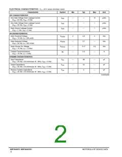
ELECTRICAL CHARACTERISTICS — continued (T = 25°C unless otherwise noted)
C
Characteristic
Symbol
Min
Typ
Max
Unit
FUNCTIONAL TESTS (In Motorola Test Fixture, 50 ohm system)
Two–Tone Common–Source Amplifier Power Gain
G
16
17
—
dB
ps
(V = 26 Vdc, P = 60 W PEP, I = 450 mA,
DD
out
DQ
f1 = 945.0 MHz, f2 = 945.1 MHz)
Two–Tone Drain Efficiency
η
36
—
—
—
40
–31
–16
17
—
–28
–9
%
dBc
dB
(V = 26 Vdc, P = 60 W PEP, I = 450 mA,
DD
out
DQ
f1 = 945.0 MHz, f2 = 945.1 MHz)
3rd Order Intermodulation Distortion
IMD
IRL
(V = 26 Vdc, P = 60 W PEP, I = 450 mA,
DD
out
DQ
f1 = 945.0 MHz, f2 = 945.1 MHz)
Input Return Loss
(V = 26 Vdc, P = 60 W PEP, I = 450 mA,
DD
out
DQ
f1 = 945.0 MHz, f2 = 945.1 MHz)
Two–Tone Common–Source Amplifier Power Gain
G
—
dB
ps
(V = 26 Vdc, P = 60 W PEP, I = 450 mA,
DD
out
DQ
f1 = 930.0 MHz, f2 = 930.1 MHz and f1 = 960.0 MHz,
f2 = 960.1 MHz)
Two–Tone Drain Efficiency
η
—
—
—
39
—
—
—
%
dBc
dB
(V = 26 Vdc, P = 60 W PEP, I = 450 mA,
DD
out
DQ
f1 = 930.0 MHz, f2 = 930.1 MHz and f1 = 960.0 MHz,
f2 = 960.1 MHz)
3rd Order Intermodulation Distortion
IMD
IRL
–31
–16
(V = 26 Vdc, P = 60 W PEP, I = 450 mA,
DD
out
DQ
f1 = 930.0 MHz, f2 = 930.1 MHz and f1 = 960.0 MHz,
f2 = 960.1 MHz)
Input Return Loss
(V = 26 Vdc, P = 60 W PEP, I = 450 mA,
DD
out
DQ
f1 = 930.0 MHz, f2 = 930.1 MHz and f1 = 960.0 MHz,
f2 = 960.1 MHz)
Power Output, 1 dB Compression Point
P
—
—
—
70
17
51
—
—
—
W
dB
%
1dB
(V = 26 Vdc, P = 60 W CW, I = 450 mA,
DD
out
DQ
f1 = 945.0 MHz)
Common–Source Amplifier Power Gain
G
ps
(V = 26 Vdc, P = 60 W CW, I = 450 mA,
DD
out
DQ
f1 = 945.0 MHz)
Drain Efficiency
η
(V = 26 Vdc, P = 60 W CW, I = 450 mA,
DD
out
DQ
f1 = 945.0 MHz)
Output Mismatch Stress
(V = 26 Vdc, P = 60 W CW, I = 450 mA,
f = 945.0 MHz, VSWR = 10:1, All Phase Angles at Frequency
of Tests)
Ψ
DD
out
DQ
No Degradation In Output Power
MOTOROLA RF DEVICE DATA
MRF9060R1 MRF9060SR1
3

 MOTOROLA [ MOTOROLA ]