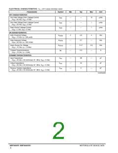
ELECTRICAL CHARACTERISTICS (T = 25°C unless otherwise noted)
C
Characteristic
OFF CHARACTERISTICS
Zero Gate Voltage Drain Leakage Current
Symbol
Min
Typ
Max
Unit
I
—
—
—
—
—
—
10
1
µAdc
µAdc
µAdc
DSS
(V = 65 Vdc, V = 0 Vdc)
DS
GS
Zero Gate Voltage Drain Leakage Current
(V = 26 Vdc, V = 0 Vdc)
I
DSS
DS
GS
Gate–Source Leakage Current
(V = 5 Vdc, V = 0 Vdc)
I
1
GSS
GS
DS
ON CHARACTERISTICS
Gate Threshold Voltage
V
V
2
2.9
3.7
4
Vdc
Vdc
Vdc
S
GS(th)
GS(Q)
DS(on)
(V = 10 Vdc, I = 200 µAdc)
DS
D
Gate Quiescent Voltage
(V = 26 Vdc, I = 450 mAdc)
—
—
—
—
0.4
—
DS
D
Drain–Source On–Voltage
(V = 10 Vdc, I = 1.3 Adc)
V
0.17
5.3
GS
D
Forward Transconductance
(V = 10 Vdc, I = 4 Adc)
g
fs
DS
D
DYNAMIC CHARACTERISTICS
Input Capacitance
(V = 26 Vdc 30 mV(rms)ac @ 1 MHz, V = 0 Vdc)
DS
C
—
—
—
98
50
2
—
—
—
pF
pF
iss
GS
Output Capacitance
(V = 26 Vdc 30 mV(rms)ac @ 1 MHz, V = 0 Vdc)
DS
C
oss
GS
Reverse Transfer Capacitance
C
pF
rss
(V = 26 Vdc 30 mV(rms)ac @ 1 MHz, V = 0 Vdc)
DS
GS
(continued)
MRF9060R1 MRF9060SR1
2
MOTOROLA RF DEVICE DATA

 MOTOROLA [ MOTOROLA ]