Freescale Semiconductor, Inc.
To insure that silicon pressure sensors are designed and
product when very few or no failures occur. With cost as a
predominant factor in any industrial setting and time of the
utmost importance, the reliability test must be optimized.
Optimization of reliability testing will allow the maximum
amount of information on the product being tested to be
gained in a minimum amount of time, this is accomplished by
using accelerated life testing techniques.
A key underlying assumption in the usage of accelerated
life testing to estimate the life of a product at a lower or
nominal stress is that the failure mechanism encountered
at the high stress is the same as that encountered at the
nominal stress. The most frequently applied accelerated
environmental stress for semiconductors is temperature, it
will be briefly explained here for its utilization in deter-
mining the lifetime reliability statistics for silicon pressure
sensors.
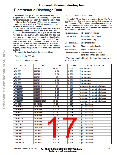
manufactured for reliability, an in-depth insight into what
mechanisms cause particular failures is required. It is safe to
say that unless a manufacturer has a clear understanding of
everything that can go wrong with the device, it cannot
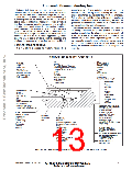
design a device for the highest reliability. Figure 2 provides a
look into the sensor operating concerns for a variety of
potential usage applications. This information is utilized
when developing the Failure Mode and Effects Analysis
(FMEA). The FMEA then serves as the documentation that
demonstrates all design and process concerns have been
addressed to offer the most reliable approach. By under-
standing how to design products, control processes, and
eliminate the concerns raised, a reliable product is achieved.
ACCELERATED LIFE TESTING
It is very difficult to assess the reliability statistics for a
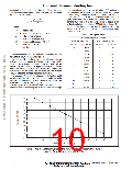
SENSOR RELIABILITY CONCERNS
DIE
GEL:
Viscosity
Thermal Coefficient of Expansion
Permeability (Diffusion x Solubility)
Changes in Material or Process
Height
Coverage
Uniformity
PACKAGE:
Integrity
Plating Quality
Dimensions
Thermal Resistance
Mechanical Resistance
Pressure Resistance
Media Compatibility
METALLIZATION:
Lifting or Peeling
Alignment
Scratches
Voids
Laser Trimming
Thickness
Step Coverage
Contact Resistance Integrity
Adhesive Properties
Media Compatibility
Gel Aeration
DIAPHRAGM:
Size
Compressibility
Thickness
Uniformity
Pits
Alignment
Fracture
PASSIVATION:
Thickness
Mechanical Defects
Integrity
BONDING WIRES:
Strength
Placement
Height and Loop
Size
Material
Bimetallic Contamination
(Kirkendall Voids)
Nicking and other damage
General Quality & Workmanship
Uniformity
ELECTRICAL PERFORMANCE:
Continuity and Shorts
Parametric Stability
Parametric Performance
Temperature Performance
Temperature Stability
Long Term Reliability
Storage Degradation
LEADS:
Materials and Finish
Plating Integrity
Solderability
General Quality
Strength
Contamination
Corrosion
Adhesion
MARKING:
Permanency
Clarity
DIE ATTACH:
Uniformity
Susceptibility to Radiation Damage
Design Quality
Resistance to Mechanical Stress
Resistance to Temperature Stress
Wetting
Adhesive Strength
Cohesive Strength
Process Controls
DESIGN CHANGES
MATERIAL OR PROCESS
CHANGES
FAB & ASSEMBLY CLEANLINESS
SURFACE CONTAMINATION
FOREIGN MATERIAL
SCRIBE DEFECTS
DIFFUSION DEFECTS
OXIDE DEFECTS
Die Orientation
Die Height
Change in Material or Process
Media Compatibility
Compressibility
Figure 2. Process and Product Variability Concerns During Reliability Testing
Motorola Sensor Device Data
www.motorola.com/semiconductors
Go to: www.freescale.com
1–7
For More Information On This Product,

 MOTOROLA [ MOTOROLA ]