ELECTRICAL CHARACTERISTICS (T = 25 C unless otherwise noted)
C
Characteristic
Symbol
Min
Typ
Max
Unit
OFF CHARACTERISTICS
(1)
Collector–Emitter Sustaining Voltage
(I = 2.5 mAdc, I = 0)
V
350
—
—
—
—
—
—
—
0.25
0.5
0.1
0.1
Vdc
CEO(sus)
C
B
Collector Cutoff Current
(V = 250 Vdc, I = 0)
I
mAdc
mAdc
mAdc
mAdc
CEO
CE
Collector Cutoff Current
(V = 375 Vdc, V
B
I
—
CEX
= 1.5 Vdc)
CE EB(off)
Collector Cutoff Current
(V = 375 Vdc, I = 0)
I
—
CBO
CB
Emitter Cutoff Current
(V = 5.0 Vdc, I = 0)
E
I
—
EBO
BE
C
ON CHARACTERISTICS (1)
DC Current Gain
(I = 50 mAdc, V
C CE
h
FE
—
= 10 Vdc)
= 10 Vdc)
MJE2360T
MJE2361T
MJE2360T
MJE2361T
25
50
15
40
—
—
—
—
200
250
—
(I = 100 mAdc, V
C CE
—
Collector–Emitter Saturation Voltage
(I = 100 mAdc, I = 10 mAdc)
V
—
—
1.5
1.0
Vdc
Vdc
CE(sat)
C
B
Base–Emitter On Voltage
(I = 100 mAdc, V = 10 Vdc)
V
BE(on)
—
—
C
CE
DYNAMIC CHARACTERISTICS
Current–Gain — Bandwidth Product
f
—
—
10
20
—
—
MHz
pF
T
(I = 50 mAdc, V
C CE
= 10 Vdc, f = 1.0 MHz)
Output Capacitance
(V = 100 Vdc, I = 0, f = 100 kHz)
C
ob
CB
E
(1) Pulse Test: Pulse Width
300 µs, Duty Cycle
2.0%.
1.0
0.5
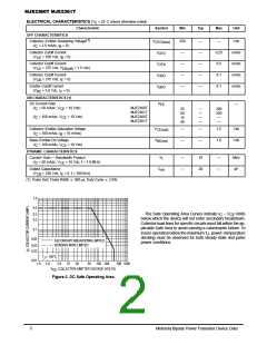
The Safe Operating Area Curves indicate I – V
limits
CE
0.3
0.2
C
below which the device will not enter secondary breakdown.
Collector load lines for specific circuits must fall within the ap-
plicable Safe Area to avoid causing a catastrophic failure. To
0.1
insure operation below the maximum T , power–temperature
J
derating must be observed for both steady state and pulse
power conditions.
0.05
SECONDARY BREAKDOWN LIMITED
BONDING WIRE LIMITED
0.03
0.02
T
= 150
°C
J
0.01
1.0
2.0
5.0
10
20
50
100 200
500 1000
V
, COLLECTOR–EMITTER VOLTAGE (VOLTS)
CE
Figure 2. DC Safe Operating Area
2
Motorola Bipolar Power Transistor Device Data

 MOTOROLA [ MOTOROLA ]