Freescale Semiconductor, Inc.
peripheral circuits for automatic wait-state insertion. These signals also interface to 8-, 16-, or 32-bit ports. In
addition, other external bus masters can access chip-selects. The upper 4 chip-selects are multiplexed with
A[27:24] of the address bus and the 4 write-enable signals. The base address, access permissions, and timing
waveforms are all programmable with configuration registers.
Except for full-page mode, all operations are available to other external bus masters. The DRAM controller can
generate CAS and RAS for an external master and can continue to manage refresh requests.
8-Bit General-Purpose Interface. An 8-bit general-purpose programmable parallel port serves as either an
input or an output on a bit-by-bit basis. The parallel port is multiplexed with PST[3:0] and DDATA[3:0] debug
signals.
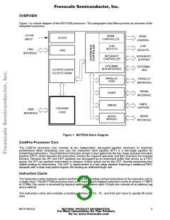
Interrupt Controller. The interrupt controller provides user-programmable control of 3 or 7 external interrupt
and 5 internal peripheral interrupts. Users can program each internal interrupt to any one of 7 interrupt levels
and 4 priority levels within each of these levels. The 3 external interrupt signals can be configured as either
fixed interrupt levels 1, 4, and 7, or as a 7-level encoded interrupt. Users can program the external interrupts
to any one of the 4 priority levels within the respective interrupt levels.
System Protection. The MCF5206 processor contains a 16-bit software watchdog timer with an 8-bit
prescaler. The programmable software watchdog timer provides either a level 7 interrupt or a hardware reset
on timeout. The MCF5206 processor also contains a reset status register that indicates the cause of the last
reset.
JTAG.To help with system diagnostics and manufacturing testing, the MCF5206 processor includes dedicated
user-accessible test logic that complies with the IEEE 1149.1 standard for boundary scan testability, often
referred to as Joint Test Action Group, or JTAG. For more information, refer to the IEEE 1149.1 standard.
System Debug Interface
The ColdFire processor core debug interface supports real-time trace and background-debug mode. A four-
pin background debug mode (BDM) interface provides system debug. The BDM is a proper subset of the BDM
interface provided on Motorola’s 683XX Family of parts.
In real-time trace, 4 status lines provide information on processor activity in real time (PST pins). A 4-bit wide
debug data bus (DDATA) displays operand data, which helps track the machine’s dynamic execution path as
the change-of-flow instructions execute. These signals are multiplexed with an 8-bit parallel port for application
development, which does not use real-time trace.
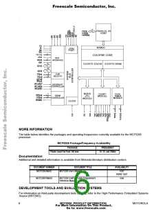
Pinout and Package
The MCF5206 device is supplied in a 160-pin plastic quad flat pack package with the pinout shown in Figure 2.
MOTOROLA
MCF5206 PRODUCT INFORMATION
5
For More Information On This Product,
Go to: www.freescale.com

 MOTOROLA [ MOTOROLA ]