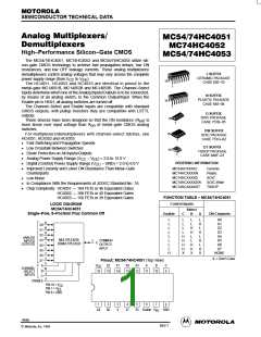
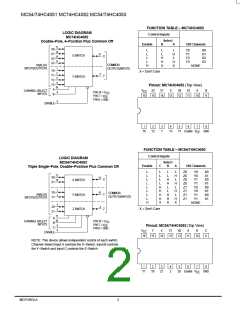
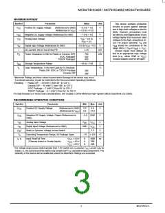
MC54/74HC4051 MC74HC4052 MC54/74HC4053
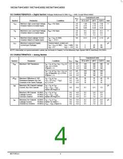
AC CHARACTERISTICS (C = 50 pF, Input t = t = 6 ns)
L
r
f
Guaranteed Limit
V
CC
V
Symbol
Parameter
Unit
–55 to 25°C
≤85°C
≤125°C
t
t
t
,
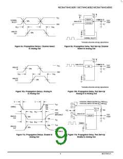
Maximum Propagation Delay, Channel–Select to Analog Output
(Figure 9)
2.0
4.5
6.0
370
74
63
465
93
79
550
110
94
ns
PLH
t
PHL
,
Maximum Propagation Delay, Analog Input to Analog Output
(Figure 10)
2.0
4.5
6.0
60
12
10
75
15
13
90
18
15
ns
ns
ns
PLH
t
PHL
,
Maximum Propagation Delay, Enable to Analog Output
(Figure 11)
2.0
4.5
6.0
290
58
49
364
73
62
430
86
73
PLZ
t
PHZ
t
t
,
Maximum Propagation Delay, Enable to Analog Output
(Figure 11)
2.0
4.5
6.0
345
69
59
435
87
74
515
103
87
PZL
PZH
C
Maximum Input Capacitance, Channel–Select or Enable Inputs
10
35
10
35
10
35
pF
pF
in
C
Maximum Capacitance
(All Switches Off)
Analog I/O
I/O
Common O/I: HC4051
HC4052
130
80
130
80
130
80
HC4053
50
50
50
Feedthrough
1.0
1.0
1.0
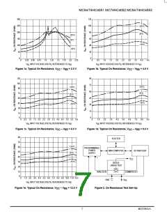
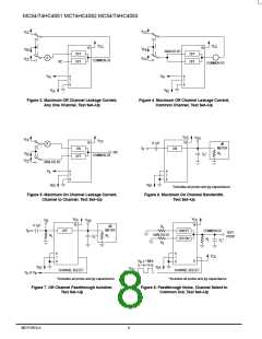
NOTE: For propagation delays with loads other than 50 pF, and information on typical parametric values, see Chapter 2 of the Motorola High–
Speed CMOS Data Book (DL129/D).
Typical @ 25°C, V
= 5.0 V, V = 0 V
EE
CC
C
Power Dissipation Capacitance (Figure 13)*
HC4051
HC4052
HC4053
pF
45
80
45
PD
2
* Used to determine the no–load dynamic power consumption: P = C
D
Motorola High–Speed CMOS Data Book (DL129/D).
V
f + I
V
. For load considerations, see Chapter 2 of the
PD CC
CC CC
High–Speed CMOS Logic Data
DL129 — Rev 6
5
MOTOROLA

 MOTOROLA [ MOTOROLA ]