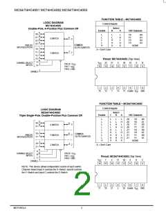
MC54/74HC4051 MC74HC4052 MC54/74HC4053
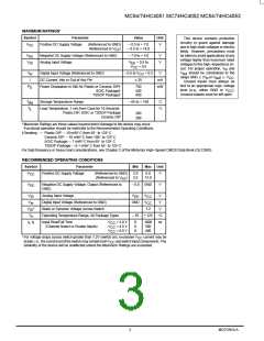
MAXIMUM RATINGS*
Symbol
Parameter
(Referenced to GND)
Value
Unit
This device contains protection
circuitry to guard against damage
due to high static voltages or electric
fields. However, precautions must
be taken to avoid applications of any
voltage higher than maximum rated
voltages to this high–impedance cir-
V
CC
Positive DC Supply Voltage
– 0.5 to + 7.0
– 0.5 to + 14.0
V
(Referenced to V
)
EE
V
Negative DC Supply Voltage (Referenced to GND)
Analog Input Voltage
– 7.0 to + 5.0
V
V
EE
V
V
V
– 0.5 to
IS
EE
+ 0.5
CC
cuit. For proper operation, V and
in
V
should be constrained to the
V
Digital Input Voltage (Referenced to GND)
DC Current, Into or Out of Any Pin
– 0.5 to V
+ 0.5
V
out
in
CC
range GND (V or V
)
V
CC
.
in out
I
± 25
mA
mW
Unused inputs must always be
tied to an appropriate logic voltage
P
D
Power Dissipation in Still Air, Plastic or Ceramic DIP†
SOIC Package†
750
500
450
level (e.g., either GND or V ).
CC
Unused outputs must be left open.
TSSOP Package†
T
Storage Temperature Range
– 65 to + 150
C
C
stg
T
Lead Temperature, 1 mm from Case for 10 Seconds
Plastic DIP, SOIC or TSSOP Package
Ceramic DIP
L
260
300
* Maximum Ratings are those values beyond which damage to the device may occur.
Functional operation should be restricted to the Recommended Operating Conditions.
†Derating — Plastic DIP: – 10 mW/ C from 65 to 125 C
Ceramic DIP: – 10 mW/ C from 100 to 125 C
SOIC Package: – 7 mW/ C from 65 to 125 C
TSSOP Package: – 6.1 mW/ C from 65 to 125 C
For high frequency or heavy load considerations, see Chapter 2 of the Motorola High–Speed CMOS Data Book (DL129/D).
RECOMMENDED OPERATING CONDITIONS
Symbol
Parameter
Positive DC Supply Voltage
Min
Max
Unit
V
CC
(Referenced to GND)
(Referenced to V
2.0
2.0
6.0
12.0
V
)
EE
V
EE
Negative DC Supply Voltage, Output (Referenced to
GND)
– 6.0 GND
V
V
Analog Input Voltage
V
V
V
V
V
IS
EE
CC
V
Digital Input Voltage (Referenced to GND)
Static or Dynamic Voltage Across Switch
Operating Temperature Range, All Package Types
GND
in
CC
V
IO
*
1.2
– 55 + 125
V
T
C
ns
A
t , t
r f
Input Rise/Fall Time
(Channel Select or Enable Inputs)
V
CC
V
CC
V
CC
= 2.0 V
= 4.5 V
= 6.0 V
0
0
0
1000
500
400
* For voltage drops across switch greater than 1.2V (switch on), excessive V
drawn;i.e., thecurrentoutoftheswitchmaycontainbothV
CC
reliability of the device will be unaffected unless the Maximum Ratings are exceeded.
current may be
CC
andswitchinputcomponents. The
High–Speed CMOS Logic Data
DL129 — Rev 6
3
MOTOROLA

 MOTOROLA [ MOTOROLA ]