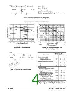
SWITCHING CHARACTERISTICS (C = 50 pF, T = 25 C)
L
A
V
Vdc
DD
Characteristic
Symbol
Min
Typ #
Max
Unit
Output Rise Time (Counter Outputs)
t
5.0
10
15
—
—
—
40
25
20
200
100
80
ns
TLH
Output Fall Time (Counter Outputs)
t
5.0
10
15
—
—
—
50
30
20
200
100
80
ns
ns
THL
Propagation Delay Time
Clock to Q4
t
t
5.0
10
15
—
—
—
415
175
125
740
300
200
PLH
PHL
5.0
10
15
—
—
—
1.5
0.7
0.4
2.7
1.3
1.0
µs
Clock to Q14
Clock Pulse Width
t
5.0
10
15
100
40
30
65
30
20
—
—
—
ns
wH
Clock Pulse Frequency
Clock Rise and Fall Time
Reset Pulse Width
f
5.0
10
15
—
—
—
5
14
17
3.5
8
12
MHz
ns
φ
t
t
5.0
10
15
TLH
THL
No Limit
t
w
5.0
10
15
120
60
40
40
15
10
ns
—
—
—
Propagation Delay Time
Reset to On
t
5.0
10
15
—
—
—
170
80
60
350
160
100
ns
PHL
#Data labelled “Typ” is not to be used for design purposes but is intended as an indication of the IC’s potential performance.
V
DD
V
DD
CLOCK
NC OUT1
PULSE
GENERATOR
500
µ
F
0.01 µF
I
D
Q4
Q5
Qn
NC OUT2
C
L
R
C
CLOCK
L
PULSE
GENERATOR
Q4
C
L
V
SS
NC OUT1 Q5
NC OUT2
Qn
C
L
R
20 ns
20 ns
C
L
C
L
V
90%
50%
10%
SS
CLOCK
t
WH
20 ns
20 ns
t
t
PLH
PHL
V
V
DD
90%
50%
10%
90%
50%
10%
CLOCK
Q
SS
t
t
THL
50% DUTY CYCLE
TLH
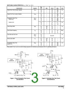
Figure 1. Power Dissipation Test Circuit
and Waveform
Figure 2. Switching Time Test Circuit
and Waveforms
MOTOROLA CMOS LOGIC DATA
MC14060B
3

 MOTOROLA [ MOTOROLA ]