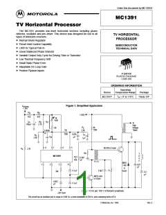
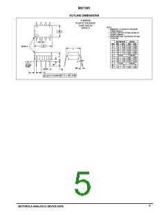
MC1391
CIRCUIT OPERATION
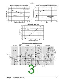
The MC1391P contains the oscillator, phase detector and
The phase detector is isolated from the remainder of the
circuit by R14 and Z2. The phase detector consists of the
comparator Q15, Q16 and the gated current source Q17.
Negative going sync pulses at Pin 3 turn off Q12 and the
current division between Q15 and Q16 will be determined by
the phase relationship of the sync and the sawtooth
waveform at Pin 4, which is derived from the horizontal
flyback pulse. If there is no phase difference between the
sync and sawtooth, equal currents will flow in the collectors of
Q15 and Q16 each of half the sync pulse period. The current
in Q15 is turned around by Q18 so that there is no net output
current at Pin 5 for balanced conditions. When a phase offset
occurs, current will flow either in or out of Pin 5. This pin is
connected via an external low–pass filter to Pin 7, thus
controlling the oscillator.
predriver sections needed for a television horizontal APC loop.
The oscillator is an RC type with one pin (Pin 7) used to
control the timing. The basic operation can be explained
easily. If it is assumed that Q7 is initially off, then the capacitor
connected from Pin 7 to ground will be charged by an
external resistor (R ) connected to Pin 6. As soon as the
C
voltage at Pin 7 exceeds the potential set at the base of Q8
by resistors R8 and R10, Q7 will turn on and Q6 will supply
base current to Q5 and Q10. Transistor Q10 will set a new,
lower potential at the base of Q8 determined by R8, R9 and
R10. At the same time, transistor Q5 will discharge the
capacitor through R4 until the base bias of Q7 falls below that
of Q8, at which time Q7 will turn off and the cycle repeats.
The sawtooth generated at the base of Q4 will appear
across R3 and turn off Q3 whenever it exceeds the bias
set on Pin 8. By adjusting the potential at Pin 8, the duty
cycle (MSR) at the predriver output pin (Pin 1) can be
changed to accommodate either tube or transistor horizontal
output stages.
Shunt regulation for the circuit is obtained with a zero
temperature coefficient from the series combination of D1,
D2 and Z1.
APPLICATION INFORMATION
–4
For a given phase detector sensitivity (µ) = 1.60 x 10 A/rad
Although it is an integrated circuit, the MC1391P has all
the flexibility of a conventional discrete component horizontal
APC loop. The internal temperature compensated voltage
regulator allows a wide supply voltage variation to be
tolerated, enabling operation from nonregulated power
supplies. A minimum value for supply current into Pin 6 to
maintain zener regulation is about 18 mA. Allowing 2.0 mA for
the external dividers
fc = µβ and β = 3.15 x R Hz/mA
C
Increasing R will raise the dc loop gain and reduce the static
C
phase error (S.P.E.) for a given frequency offset. Secondary
effects are to increase the natural resonant frequency of the
loop (ω ) and give a wider pull–in range from an out–of–lock
n
condition. The loop will also tend to be underdamped with fast
pull–in times, producing good airplane flutter performance.
However, as the loop becomes more underdamped impulse
noise can cause shock excitation of the loop. Unlimited
increase in the dc loop gain will also raise the noise bandwidth
excessively causing horizontal jitter with thermal noise. Once
the dc loop gain has been selected for adequate SPE
performance, the loop filter can be used to produce the balance
between other desirable characteristics. Damping of the loop is
V
–8.8
nonreg(min)
R
+ R =
B
A
–3
20 x 10
Components R , R and C are used for ripple rejection. If
A
B
A
the supply voltage ripple is expected to be less than 100 mV
(for a 30 V supply) then R and R can be combined and
A
B
C
omitted.
A
The output pulse width can be varied from 6.0 µs to 48 µs
achieved most directly by changing the resistor R with respect
by changing the voltage at Pin 8 (see Figure 5). However,
care should be taken to keep the lead lengths to Pin 8 as
X
to R which modifies the ac/dc gain ration (m) of the loop.
Y
Lowering this ratio will reduce the pull–in range and noise
short as possible at Pin 1. The parallel impedance of R and
D
bandwidth (fnn). (Note: very large values of R will limit the
R
should be close to 1.0 kΩ to ensure stable pulse widths.
Y
E
control capability of the phase detector with a corresponding
reduction in hold–in range.)
For 15 mA drive at saturation
V
–0.3
nonreg
–3
15 x 10
Static phasing can be adjusted simply by adding a small
resistor between the flyback pulse integrating capacitor and
ground. The sync coupling capacitor should not be too small
or it can charge during the vertical pulse and this may result in
picture bends at the top of the CRT.
R
=
F
The oscillator free–running frequency is set by R and C
C
B
connected to Pin 7. For values of R ≥ R
discharge
(R4 in
C
Figure 6), a useful approximation for the free–running
frequency is
Note: In adjusting the loop parameters, the following
equations may prove useful:
1
f
O
=
2
1 x χ Tω
R
X
RY
0.6 R C
C
C B
χ =
f
=
=
nn
4
T
χ
Proper choice of R and C will give a wide range of
C
B
oscillator frequencies – operation at 31.5 kHz for countdown
ω
ω
C = 2 π fc
C
w
n
circuits is possible for example. As long as the product R C
C B
≈ 10 many combinations of values of R and C will satisfy
c
√ (1 + )T
–4
T = Ry CC
C
B
2
Tω
the free–running frequency requirement of 15.734 kHz.
However, the sensitivity of the oscillator (β) to control–current
from the phase detector is directly dependent on the
χ
C
K =
where: K = loop damping coeffecient
4
magnitude of R , and this provides a convenient method of
C
adjusting the dc loop gain (fc).
4
MOTOROLA ANALOG IC DEVICE DATA

 MOTOROLA [ MOTOROLA ]