THERMAL CHARACTERISTICS
Characteristic
Symbol
Max
2.2
60
Unit
°C/W
°C/W
Thermal Resistance, Junction to Case
Thermal Resistance, Junction to Ambient
R
R
θJC
θJA
ELECTRICAL CHARACTERISTICS (T = 25°C and either polarity of MT2 to MT1 voltage unless otherwise noted.)
C
Characteristic
Symbol
Min
Typ
Max
Unit
Peak Blocking Current
(V = Rated V , T = 110°C)
T
= 25°C
I
—
—
—
—
10
2
mA
Volts
mA
J
DRM
D
DRM
Peak On-State Voltage
(I = 14 A Peak, Pulse Width
J
V
—
—
2
TM
GT
2 ms, Duty Cycle
2%)
TM
Gate Trigger Current (Continuous dc)
(V = 12 V, R = 100 Ω)
I
D
L
MT2(+), G(+); MT2(+), G(–); MT2(–), G(–)
MT2(–), G(+) “A” Suffix Only
—
—
—
—
5
10
Gate Trigger Voltage (Continuous dc)
V
GT
Volts
(V = 12 V, R = 100 Ω)
D
L
MT2(+), G(+); MT2(+), G(–); MT2(–), G(–)
MT2(–), G(+) “A” Suffix Only
—
—
—
—
2
2.5
(V = Rated V
All Trigger Modes
, T = 110°C, R = 10 k)
C L
D
DRM
0.2
—
—
—
—
Holding Current
(V = 12 V, I
D TM
I
15
mA
µs
H
= 200 mA, Gate Open)
Gate-Controlled Turn-On Time
(V = Rated V , I = 14 A Peak, I = 30 mA)
t
—
—
—
1.5
25
5
—
—
—
gt
D
DRM TM
Critical Rate of Rise of Off-State Voltage
(V = Rated V , Exponential Waveform, T = 110°C)
G
dv/dt
V/µs
V/µs
D
DRM
Critical Rate of Rise of Commutation Voltage
(V = Rated V , I = 14 A Peak,
C
dv/dt(c)
D
DRM TM
Commutating di/dt = 5 A/ms, Gate Unenergized, T = 80°C)
C
20
16
120
dc
180
°
110
100
12
8
120
°
90°
60°
30°
30
60
°
°
90
80
90
°
180
4
0
°
dc
0
2
4
6
8
10
0
2
I
4
6
8
10
I
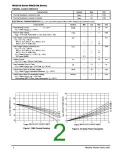
, RMS ON-STATE CURRENT (AMPS)
, RMS ON-STATE CURRENT (AMPS)
T(RMS)
T(RMS)
Figure 1. RMS Current Derating
Figure 2. On-State Power Dissipation
2
Motorola Thyristor Device Data

 MOTOROLA [ MOTOROLA ]